

nand2tetrisPart1
nand2tetrisPart1Logic diagrams for nand2tetris part 1 (projects 1 to 6).
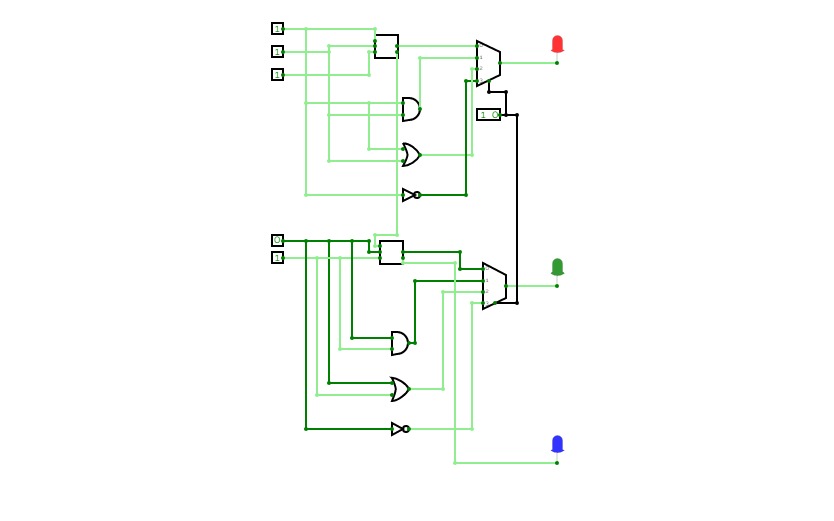
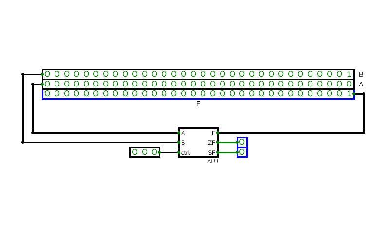
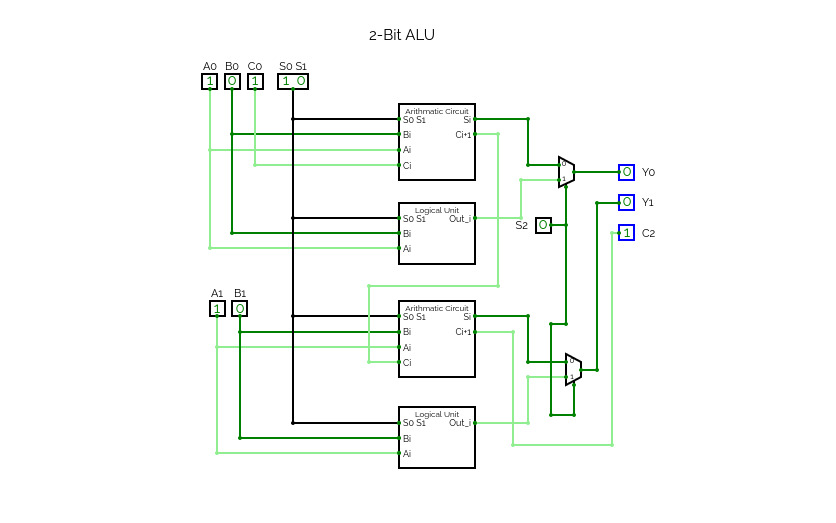
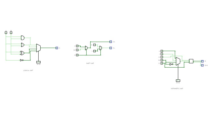
4 BIT ALU
4 BIT ALUThis is part of a project to construct a 4 BIT CPU from scratch. I will be starting with a simple NOR gate and building it up to a working model with ALU registers, RAM and ROM. I will be designing an op code and assembler to go with it. Progress and detail can be found on my blog here
This file contains the ALU

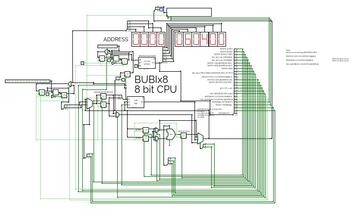
8 Bit CPU
8 Bit CPUThis is a CPU witch is capable of executing a lot of stuff in one clock cycle, and this CPU can shift left up to 7 times and shift right up to 7 times witch means that it is possible to multiply and divide in one clock cycle if you program a table in the program memory. it has a 32 bit instruction width and a 8 bit address. it also has
The ALU has the following operations:
- ADD
- SUBTRACT
- SHIFT_LEFT (up to 7 times per cycle 3 bit)
- SHIFT_RIGHT (up to 7 times per cycle 3 bit)
- XOR
- OR
- NOT
This Was made by miles

t729 CPU - old
t729 CPU - oldt729 is a 6/12-trit balanced ternary processor.
It is built with normal binary logic gates using binary encoded ternary (10, 00, 01) to create the ternary logic gates. While this probably increases complexity, I've not found a logic simulator that does ternary. I tried circuit simulators but working with negative and positive voltages with transistors is kind of a pain and very slow to design. Sure binary encoded ternary is more wire complex but it does only require one voltage and should technically use less power and run faster. Also binary logic gates are super cheap. Using binary logic gates also means the design should work on FPGAs and could in theory get manufactured as a microprocessor.
I've gone with 6-trit = 1 Tryte for my system. 12-trit / 2 Tryte is a "word".
Data and instruction width is 6-trit (729)
Address width is 12-trit (531,441)
The t729 is a hobby project I've been extremely slowly working on for a few years.
It's purely a project for fun. Completely self taught so probably a lot of doing things the wrong way.
Currently I'm mostly hung up on instruction set. It's hard choosing which instructions to have and how to implement them.
Huge thanks to http://homepage.divms.uiowa.edu/~jones/ternary/ for the ternary logic knowledge.
If you would like to add something to the project or point something out please comment or e-mail (gmail*dyne.unlimited)
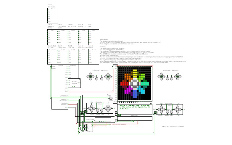

Femto-4v2.6 (Computer)
Femto-4v2.6 (Computer)A 16-bit computer/maybe console inspired thing, the Femto-4. This will be the main branch and backups will be forks from it. This project was started around November 2020.
Currently runs:
- Cart A: Flappy Bird
- Cart B: Some Pixel Art
- Cart C: Screensaver
- Cart D: Snake
- Cart E: Phemton Demonstrations
- Cart F: Competitive Snake
- Cart G: Tic Tac Toe
- Cart H: Connect 4
- Cart I: NIM
- Cart J: Bad Apple
- Bundle Cart: All carts in one
- Cart 2A: 32x32 Snake
- Cart 2B: 32x32 Competitive Snake
- Cart 2C: 32x32 Pixel Art
- Cart 2D: 32x32 Bad Apple
- Bundle Cart 2: All 32x32 carts in one
Assembler:
Compiler:
- https://github.com/Comerstar/PhemtonCompiler/blob/main/PhemtonLiteCompiler/PhemtonDeveloperGuide.txt
The 256-Series:
Full screen Notes:
For some reason, the Femto-4v2.6 only is having issues around caching previous subcircuits. Should you need to use something to unbind key entries from the full screen button, toggle the clock. Previous versions are completely unaffected.
Cart Notes:
Cart A:
- The first cart written for the Femto-4.
Cart B:
- The sprites in the cart are:
- A: Femto-4 Logo.
- B: Madeline from Celeste.
- C: Madeline from Celeste (again).
- D: Part of you aka Badeline from Celeste.
- E: A strawberry from Celeste.
- F: Standing Mario from Super Mario Bros.
- G: Jumping Mario from Super Mario Bros.
- H: Standing Mario from Super Mario Bros 3.
- I: Running Mario from Super Mario Bros 3.
- J: Sanderokian (my own character).
Cart C:
- Enter anything into the keyboard to randomise the colours.
- Enter r into the keyboard to reset the colours.
Cart D:
- WASD Pad is recommended.
- Game settings (enter the letter before starting the game to use the setting):
- e: toggle whether crashing into the edges results in a game over.
- The two modes (with/without edge collisions) have two separate high scores.
- w: change the snake's colour scheme to white.
- r: change the snake's colour scheme to red.
- y: change the snake's colour scheme to yellow.
- o: change the snake's colour scheme to orange.
- p: change the snake's colour scheme to purple.
- a: change the snake's colour scheme to aqua.
- g: change the snake's colour scheme to green.
- b: change the snake's colour scheme to blue.
- m: change the snake's colour scheme to magenta.
- 1: change the snake's colour scheme to pink.
- 2: change the snake's colour scheme to light blue.
- 3: change the snake's colour scheme to the challenge colour scheme with an invisible body.
- 0: randomise the snake's colour scheme.
Cart E:
- The test codes in the cart are:
- 1: Hello World.
- 2: Single Operator Calculator.
- 3: Exponentiation Calculator.
- 4: Fibonacci Calculator.
- 5: Keyboard to TTY Test.
- 6: Keyboard to TTY LDI LID Test.
- 7: Keyboard to TTY LII Test.
- 8: Keyboard to TTY LIA Test.
Cart F:
- WASD Pad is essentially required.
- Game settings (enter the letter before starting the game to use the setting):
- e: toggle whether crashing into the edges results in a game over.
- w: toggle whether the number of wins each player has is tracked.
- s: toggle whether the total score each player has scored is tracked.
- d: display the total wins and total scored.
- r: reset the tracked statistics.
Cart G:
- The small light in the corner indicates which player's turn it is.
- When it is dimmed, it means that the computer is processing that player's turn.
- Game settings (enter the letter before starting the game to use the setting):
- w: toggle whether the number of wins each player has is tracked.
- s: toggle automatic start player swapping. d: display the wins each player has.
- r: reset the wins each player has.
Cart H:
- The bar at the top indicates which player's turn it is.
- When it is dimmed, it means that the computer is processing that player's turn.
- Game settings (enter the letter before starting the game to use the setting):
- w: toggle whether the number of wins each player has is tracked.
- s: toggle automatic start player swapping.
- d: display the wins each player has.
- r: reset the wins each player has.
Cart I:
- Game settings (enter the letter before starting the game to use the setting):
- w: toggle whether the number of wins each player has is tracked.
- s: toggle automatic start player swapping.
- d: display the wins each player has.
- r: reset the wins each player has.
- i: display the game instructions.
- c: toggle the whether player 2 is played by the computer.
Cart J:
- Plays Bad Apple
- There are no further controls
Cart 2A:
- The options are the same as Cart D.
Cart 2B:
- The options are the same as Cart F.
Cart 2C:
- The sprites in the cart are:
- A: Femto-4 Logo.
- B: Sanderokian (my own character).
- C: Alstran (my own character).
Cart 2D:
- Plays Bad Apple on the larger screen
- There are no further controls
Features:
- Immediate, direct, & indirect memory access.
- Jumps & conditional jumps.
- 16-bit address space.
- Switchable memory banks, allowing for a standard cart to hold up to 1MB of data.
- An ALU capable of logical operators, addition, subtraction, shift left, shift right, multiplying, dividing, & other specialised functions.
- Fast execution - can run more than one instruction per clock cycle.
- 16x16 pixel display with 32 sprites and 15-bit direct colour.
- 32x32 pixel display with 32 sprites which can have up to 18-bit direct colour.
- Two controllers, a keyboard mapping for the controllers, & a keyboard for text inputs.
- RNG, TTY, stack, & save memory.
- Von Neumann Architecture.
- Assembler & compiler (written in Python).
- Twelve pre-written carts to play with.
Updates:
v1.0:
- Finished the project and added Cart A.
v1.1:
- Added Cart B, some Pixel Art.
- Fixed GRF, & AXR instructions.
- Made Bootloader clear TTY, Keyboard, & Controller Pushed.
- Updated Cart A & Cart B to make use of AXR instructions.
v1.2:
- Added Cart C, a Screensaver.
- Updated Cart B to respond to the start button on both controllers.
v1.3:
- Added Cart D, Snake.
- Moved to new project to fix issues around searching for projects branched from private projects.
- Removed unnecessary EEPROM banks and write lines from all carts.
- Made Reset clear WRAM and the General Registers.
v1.4:
- Fixed Keyboard.
- Added a Bundle Cart that allows you to view all the carts without changing carts (you must reset the console to view another cart).
- Fixed bug in the standard bank design which wrote data to incorrect addresses.
- Fixed contention issue in Mult.
- Added Annotations to the In Debug.
v1.5:
- Added Snake Player.
- Added Reset & Power labels to the relevant buttons.
v2.0:
- Further optimisation to reduce lag/increase execution speed.
- Added more memory access options.
v2.1:
- Further optimisation of the CU.
- Added a keyboard to controller mapping.
v2.2:
- Continued optimisation and overhaul of the CU.
- Removed old CU & compare circuits.
- Added additional stack access instructions.
- Updated the debug versions with the changes, as well as fixing bugs in the debug versions.
- Designed a Logo for the Femto-4.
- Rewrote Cart C to allow the sprites to be viewed in any order, and added the logo to it.
v2.3:
- Introducing Phemton Lite, the first version of the Femto-4's high level languages.
- Added a link to Phemton Lite's compiler.
- Added Cart E to demonstrate code written in Phemton Lite.
- Combined SpecialD & ROMD1, and removed SpecialD & ROMDB.
- Updated Snake code & Bundle code to match the new addresses.
- Added Cart F, a competitive version of Snake.
- Added an additional sprite into Cart B.
- Fixed issues with LII, LXA & LXP instructions.
v2.4:
- Fixed alignment of the upper carts.
- Added Cart G & Cart H, Tic Tac Toe & Connect 4 written in Phemton Lite.
- Added progress lights to Cart G & Cart H.
- Reworked bundle cart to make the code shorter and more efficient for large numbers of carts.
- Made Cart G & Cart H faster.
- Reshuffled Cart E test codes and added 2 Cart E test codes, exponentiation & Fibonacci calculation.
- Added game options to Cart D, Cart F, Cart G, & Cart H.
- Updated Cart C to allow the colours to be randomised.
- Added optional colour schemes for Cart D.
- Fixed Snake Player.
- Remade the multiply and divide circuits to take advantage of the inbuilt adders.
- Removed old MultM and DivM circuits.
v2.5:
- Further optimisation of the CU.
- Optimisation of the fast execution clocks for the computer, the graphics, & the WASD Pad.
- Fixed debug versions' issues with Phemton conditionals and added optimisations to the debug versions.
- Added 32x32 screen PPU.
- Added Cart 2A, Cart 2B, & Cart 2C, 32x32 versions of Snake, Competitive Snake, & Pixel Art.
- Added Cart I, NIM written in Phemton Lite.
v2.6
- Added the ability to directly write sprites to the PPU during execution.
- Significantly optimised the CU by removing unnecessary subcircuits.
- Introduced significant quantities of lazy evaluation to further improve performance.
- Added Cart J, and Cart 2D, which both play Bad Apple.
- The Femto-4 can now be added to the set of things that plays Bad Apple.
Future Updates:
- More pre-written carts.
- Bug fixes.
- Adding an optimiser to the compiler.
- Phemton Full.
- Phemton Plus.
Do fork the project and write your own code for it! If you want more information on how to do so read the Developer Guide in the assembler.
Note: The Flappy Bird high score and the Snake high score are mine. If you want to save your own scores permanently you will have to fork the project.
The Femto-4

General Architecture: The Femto-4 is a 16-bit, Von Neumann architecture computer with variable length instructions that are comprised of multiple 16-bit words. It has many features associated with CISCs, such as variable length instructions, and multicycle indirect loads, however operates like a RISC, with each instruction taking exactly 1 clock cycle. This was done to give the Femto-4 power whilst keeping its construction simple. First the OP code of the instruction is read, and then depending on the OP code, additional pieces of data may be read for the operands. This allows execution to become incorrectly offset, which can lead to the execution of garbage if the PC is jumped to an incorrect address. This is usually fine, since the OP code space is so empty that the data will likely be passed one at a time until the next valid instruction. Instructions are read from main memory, making this architecture a Von Neumann architecture as opposed to a Harvard architecture. The MAR always specifies the address being read to or written from, whilst the MDR always holds the data being written. Data from the data out bus can be written to most special registers during the instruction. OP codes and operands are all 16-bits. The large OP code size was chosen due to the high number of ALU instructions. There are approximately 500 interpretable OP codes that the computer can handle.
Memory Mapping: The 16-bit address space of the Femto-4 is memory mapped, with all data being stored somewhere in the address space. The last 48kx16b of memory (all addresses starting with 0b01, 0b10, or 0b11) are dedicated to the cart memory. This is where the interchangeable program would be stored, allowing programs to be easily changed by changing carts. The carts have 32 16kx16b EEPROM/RAM chips, which can be switched between during execution by writing to address 0x00cc. This gives each cart 512kx16b of memory to play with. In theory, additional memory can be added in a cart by creating a similar system on the inside of the cart, which would allow it to swap between even more EEPROM/RAM chips. The initial 16kx16b are therefore mapped to everything else, including a fixed WRAM chip that cannot be switched out, the bootloader, the PPU data, general registers, the stack, inputs, outputs, and a few special registers, such as the protect, mode, and flag registers.
Fast Execution: Execution at the fastest clock speed (one pulse every 100ms, or 10Hz, which is defined as the clock changing state every 50ms, or at a rate of 20Hz) is terribly slow, and would make reasonable graphics effectively impossible. Due to this, the Femto-4 includes several execution modes that allow the computer to run much faster. There are two registers involved in this, address 0x00ca, the mode register, and address 0x00cb, the protect register. When the two least significant bits of the mode register are low, the computer runs normally, executing 1 instruction per clock pulse. When bit 0 is set high, the computer enters fast execution on the rising edge, where it executes multiple instructions per clock pulse. This is achieved by looping an inverter into itself, producing a loop that will pulse indefinitely until the looping line is stopped by some external factor. Stopping the loop is critical since leaving the loop running will stop CircuitVerse's execution, due to it going over the stack limit of the execution. Fast execution is always paused by a 0x0000 and 0x0001 OP Code. Bit 2 enables falling edge fast execution, which can be done with rising edge fast execution producing dual edge fast execution. Setting the third bit of the mode register high will enable protection. This will ensure that computer only executes as many instructions as the value in the protect register. This protects execution by ensuring that the loop will always pause before the cycle limit is reached. Since some operations are far more complex than other operations, the maximum number of instructions per clock pulse is variable, and testing should always be conducted to ensure that the limit is not reached. Due to this, for games that need regular graphics updates, it is recommended that protection is not used, and instead the pauses are fully code controlled. On the other end of the mode register are the graphics mode. The highest two bits give the graphics update mode, 0b00 for falling edge only (normal speed), 0b01 for dual edge (double speed), 0b10 for every other clock pulse (half speed), and 0b11 for code controlled, where the 0x0001OP Code is required to update the graphics. The third most significant bit is the graphics disable bit. Setting it high stops updating the graphics, reducing lag by prevent the graphics fast execution loop from running. The mode and protection values are only updated on the rising edge of the clock pulse, and therefore there should always be pauses before and after any execution mode or protection change. By default, the Femto-4 executes with a protection value of 16, to allow the carts to run smoothly, however, depending on the instructions being used, that number can be raised to 64.
Graphics (16x16): The Femto-4 is capable of driving a 16x16 15-bit direct colour screen. It has space for 32 sprites which are rectangles with an assigned colour. All the sprites are drawn to the screen whenever a graphics update occurs, depending on the graphics mode. When using dual-edge fast execution, the falling edge should only be used to execute game code, since writing graphics data as the screen is being drawn may mess up the graphics. These 32 sprites have their data stored in the PPU RAM in the following format: The first 16 bits are the corners of the rectangle, with each coordinate being 4 bits. The coordinates are ordered x coordinate 1 (4), x coordinate 2 (4), y coordinate 1 (4), y coordinate 2 (4). The second coordinates are offset up by 1, to allow the full screen to be drawn to, such that the dimensions of the rectangle are (x2 - x1) + 1 and (y2 - y1) + 1. The next 16 bits are the sprites colour, with the first 15 bits being used for 15-bit direct colour, and the last bit being used to enable or disable drawing the sprite. The last bit is important to ensure that blank sprites are not drawn to the screen. Since the screen is not wiped every time it is refreshed, the background must be a sprite to ensure that the screen is fully wiped before the rest of the sprites are drawn on. Control of this allows carts to draw a single frame over multiple updates, allowing the 32-sprite limit to be bypassed (see how Snake works). The sprites are drawn in memory order, with the sprite with the largest address always being drawn last and therefore on top, of all other sprites. This is achieved by using the exact same system as fast execution, which reads off all the sprite data and draws them to the screen in a single clock pulse. This can loop more times safely than the main CPU since it has less dependencies which dramatically decreases the simulation's stack usage.
Graphics (32x32): The Femto-4 can also drive a 32x32 screen, with sprites able to be drawn through 3 different modes. The 32x32 screen PPU treats the addresses as one combined 32-bit value, with the value with the smaller address going first. The first 3 bits of the 32 bits define the mode. Only the values 1, 2, 3, correspond to actual sprites, whilst the rest are not drawn to the screen. Mode 1 splits the remaining 29-bit space as the following: unused (1), x coordinate (5), y coordinate (5), red (6), green (6), blue (6). Mode 2 splits the 29-bit space in the following way: x coordinate 1 (5), x coordinate 2 (5), y coordinate 1 (5), y coordinate 2 (5), red (3), green (3), blue (3). Mode 3 splits the 29-bit space in the following way: unused (3), x coordinate (5), y coordinate (5), red (5), green (5), blue (5), alpha/transparency (1). As with the 16x16 screen, Mode 2's second coordinates are offset by 1 resulting in rectangles having the dimensions of (x1 - x2) + 1 and (y1 - y2) + 1. Mode 3 is designed to allow the colours used in the 16x16 screen to be the same, making converting code between the two versions easier. The update mechanism is the same as 16x16 screen.
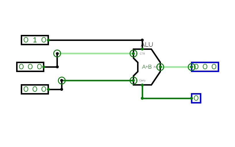
ALU: The basic ALU was inspired by the ALU-74LS181. It was designed to flexibly change between various operations by changing an additional piece of data which is bundled in the OP code. This allows a single ALU to handle all the required processes, such as the basic binary logic operations, shift left, adding, and subtracting, reducing the number of circuits required, as well as the logic required to decide which instruction to use. The Femto-4 also can multiply, divide, shift right, shift left/right by a specified number of bits, and perform operations designed to work with the computer's graphics data.
Conditional Jumps: The Femto-4 can perform immediate and direct jumps depending on the flags, a specified bit of the accumulator, and the clock. The flag jumps allow for comparisons to be made. There are three flags, the carry, the most significant bit in the accumulator, and if the accumulator value is 0, the equals flag. By performing A-B, we can compare A and B by looking at the flags. If the equals flag is true, then A=B, since A-B = 0. If the most significant bit is 0, then the number is positive or 0 (by two's complement) and therefore A>=B. The comparison is not entirely correct for numbers in two's complement (a large positive number and a large negative number when subtracted can yield a positive number), but for small values it works well. Whilst we cannot directly check A<=B using A-B in this design, we can simply flip the subtraction to B-A to do so. The accumulator bit testing is mainly used to check for controller inputs. Since each button in the controller is mapped to one bit, bit testing that bit effectively allows us to check if a button has been pressed. A similar test could be performed using an AND instruction, and checking if the result is equal to 0 or not. Bit testing is most useful for testing an input from both controllers, since it can cut out an additional instruction. The jump on clock is there to ensure that we can jump execution on the right clock pulse, which ensures that graphics can be updated on the edge of execution.
Timing: The computer is timed using several standard delay chips. The pulse length running in to the computer is about 10k units long. Therefore, different parts an instruction are separated by 20k unit delays. Further control of timings inside these periods is achieved through 1k "On Delays", which have a 1k delay turning on, but a 0k delay turning off, ensuring that pulses do not bleed into the next pulse. These pulses can tell registers to write and what source to write from, enable the read and write lines, update the ALU, and update the stack Each instruction is separate by 600k of delay in fast execution. For more information on how delay works see here: https://circuitverse.org/users/4699/projects/circuitverse-delay-introduction.
Keyboard Mapping: The Femto-4's keyboard controller mapping was created using a specialised chip. This chip used the fast execution loop to take 15 inputs from a keyboard and map the inputs to button presses on the controllers. Since the buttons are updated several times in a clock pulse, the keyboard controller cannot handle held buttons. The keyboard mapping is designed to work with both controllers, allowing two player games to be feasible on the computer.
Assembly: The Femto-4 has an assembler that converts assembly written in a .txt into hex values in a .txt that can be copied and loaded into the EEPROM banks for storage. The assembler can handle symbol assignment, as well as assigning addresses in the code symbols to make handling jumps easier. For full details on the Femto-4's assembly language view the assembly developer guide.
Phemton: Phemton is the Femto-4's high level language, with a compiler to compile it's code into Femto-4 assembly. Phemton handles variable memory assignment, basic array assignment, if, elif, else statments, while loops, for loops, and functions. Phemton Lite is the only compiler complete, and lacks an optimiser. Phemton Lite has the concept of local scope only when compiling. All uniquely identified variables are given a global address. This reduces the runtime load since the computer does not need to decide where the variables need to go during run time. Future planned additions include generated code optimisations and optimisers, Phemton Full, which has dynamic memory assignment, and Phemton Plus, which adds additional types for floats and longs. For more details view Phemton's developer guide.
Other Notes: The memory wrappers allow external chips to interact with the main data control system, in this case used for RNG, controllers, the keyboard, and driving the text output. This makes it easy to additional chips to the computer. All assembly and Phemton code can be found in the project for the Femto-4's assembler and compiler respectively. The save data cart must be located outside of the Femto-4 circuit to ensure that its contents are automatically saved. Sorry about all the copies of this computer clogging up the top of the search results.
For more information, please read the developer guide found in the Femto-4's Assembler, or just post a comment and ask me.
This is a secret to everybody, unless you found it.

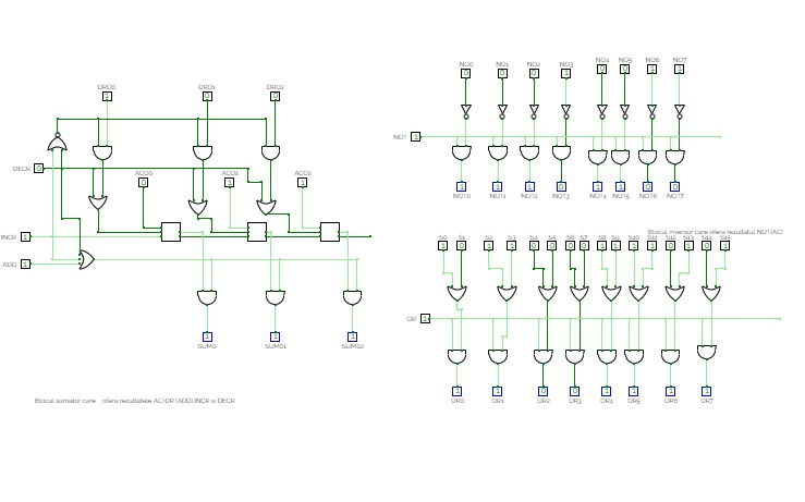
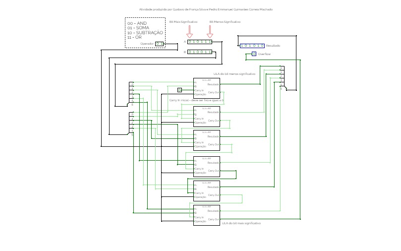
Actividad 2
Diseño de un ALU de 4 bits que realiza estas operaciones:
- AND
- OR
- Suma
- Resta
El diseño fue realizado con apoyo del libro "Computer Organization and Design" de Patterson y Henessy.
En particular resultó de ayuda el Anexo A5: Constructing a basic arithmetic logic unit.


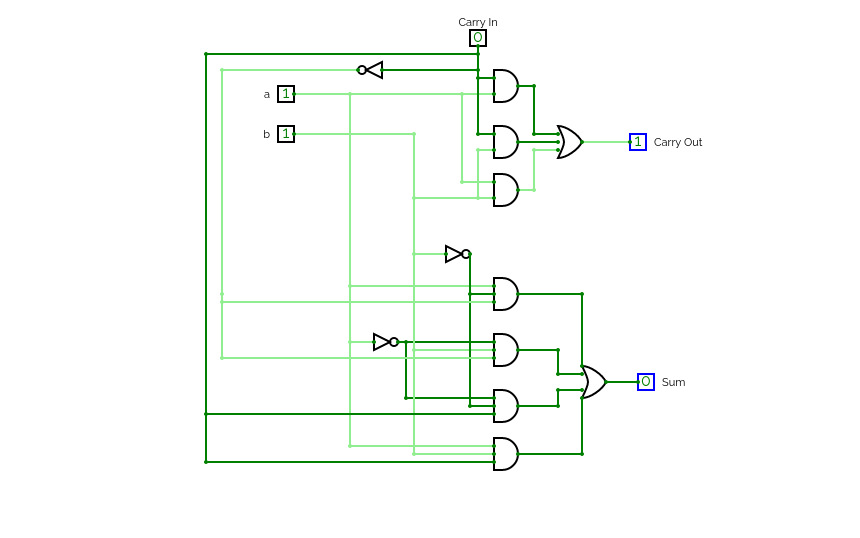
ACE mkI ALU board
ACE mkI ALU boardalu for my ACE MkI computer
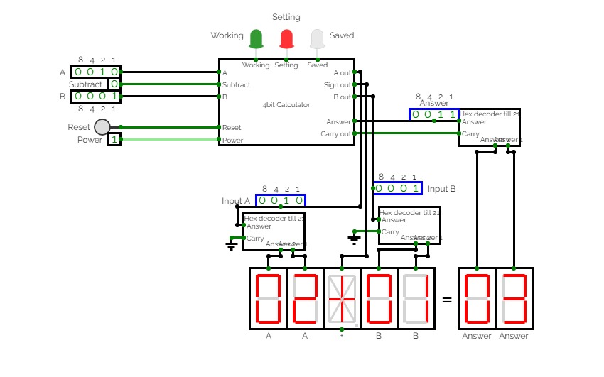
4bit Calculator
4bit CalculatorJust an 4bit calculator made for fun and learning. Used the Alu in 4bit and made a 4bit Reg to safe numbers that the alu can calculate.
ALU+ROM
ALU+ROMImplementar una ALU de 2 bits de entrada (usar la predefinida en la sección MISC del software), emplean los bits del registro de la siguiente forma:
- Usar los bits 2:4 para el código de operación
- Usar los bits 0:1 para el número B
- Usar los bits 6:7 para el número A
Luego incluir una memoria ROM de 16 byte y realizar las siguientes operaciones, en orden y visualizarlas con un contador:
- 2+3
- 1-2
- 3|1
- 1-3
- 3|~2
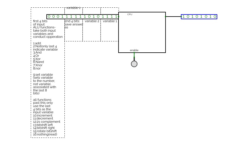
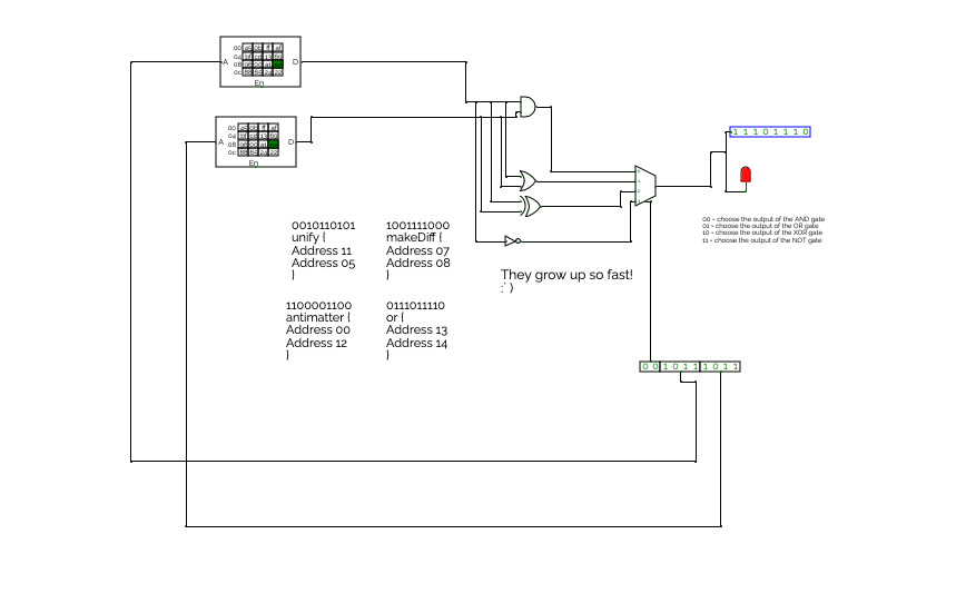
A CPU! this took me a while to figure out, mostly how to get it to run comands, but I eventually found a solution of using 4 bits as function indicators, 4 as where to save the output, 4 as the 2nd input, and 4 as the first input!
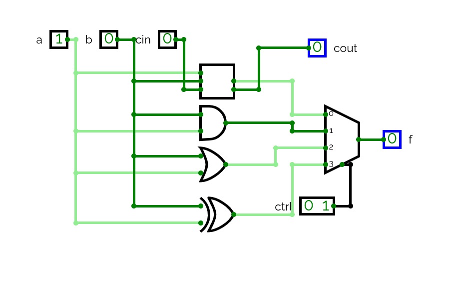
ALU
ALU
t729 - Balanced Ternary CPU
t729 - Balanced Ternary CPUt729 is a 6/12-trit balanced ternary processor.
It is built with normal binary logic gates using binary encoded ternary (10, 00, 01) to create the ternary logic gates. While this probably increases complexity, I've not found a logic simulator that does ternary.
I've gone with 6-trit = 1 Tryte for my system. 12-trit / 2 Tryte is a "word".
Data and instruction width is 6-trit (729)
Address width is 12-trit (531,441)
The t729 is a hobby project I've been extremely slowly working on for a few years.
It's purely a project for fun. Completely self taught so probably a lot of doing things the wrong way.
Currently I'm mostly hung up on instruction set. It's hard choosing which instructions to have and how to implement them.
Huge thanks to http://homepage.divms.uiowa.edu/~jones/ternary/ for the ternary logic knowledge.
If you would like to add something to the project or point something out please comment or e-mail (gmail*dyne.unlimited)

rixis combinox r1 cpu computer
rixis combinox r1 cpu computerAbout the Combinox R1:
This is the third 16-bit CPU I have made. Its new name was inspired by the new combinational code. It is also my first computer to feature a graphics and base ten display. As a result of its brand new architecture, code, and clock it is much faster than my previous CPUs.
Directions for use:
Choose the desired EEPROM program and insert it into the slot. First press the "RESET" button. Now press the "ON" button and enjoy your program.
Descriptions of programs:
blank: A blank EEPROM to be coded.
count up forever: Counts up by one until it reaches 65,535 then loops back to 0.
2+2: adds 2+2 and displays the output to the number display
transfer from keyboard to display: Displays the ascii value of whatever key is being entered on the keyboard.
random noise: Displays random noise on the screen.
Fibonacci: calculates the Fibonacci sequence
Credits:
Sanderokian Stfetoneri - clock
Sanderokian Stfetoneri - 16 bit division
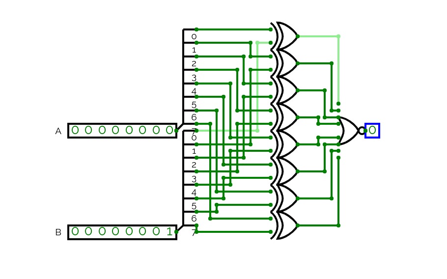

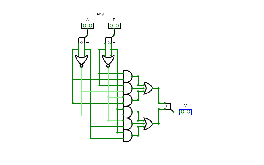
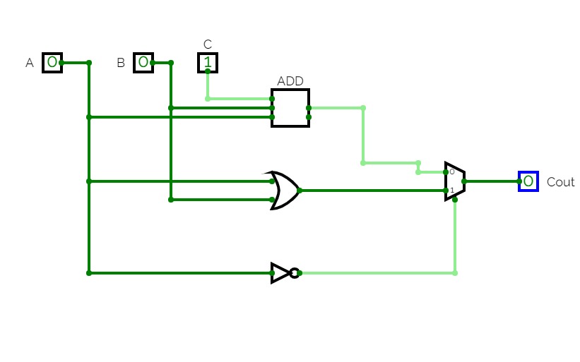
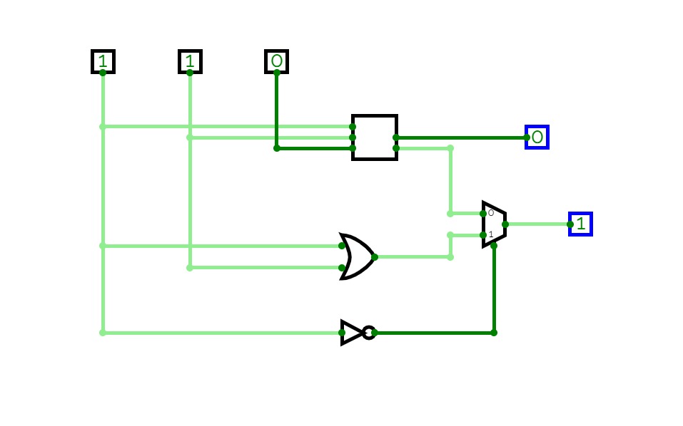
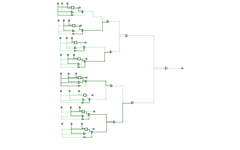
Equality Comparison (8-bit)
Equality Comparison (8-bit)


please read instructions before use
alu neutral instructions:
A IN/A OUT:0=take inputted a,1=save current output and use it as a until turned back to zero
B IN/B OUT:0=take inputted b,1=save current output and use it as b until turned back to zero
ALU SELECTION:0=take gate alu as output,1=take operation alu as output
DISPLAYS:
TOP 3=the systems current a
MIDDLE 3=output
BOTTOM 3=the systems current b
gate alu instructions:
GATE SELECTION:00=A AND B,01=A OR B,10=NOT A/B,11=A XOR B
A/B IN FOR NOT:0=take a as input for NOT,1=take b as input for NOT
operation alu instructions:
OPERATION SELECTION:0=A+B,1=A-B
SAVE A:put this alus current output in register a
SAVE B:put this alus current output in register b
OUT ALU:take output from alu
OUT A:take output from register a
OUT B:take output from register b


these notes are important please read them:
how to input code:
to input code please put your desired opcode into the computer on page "main", if you see that your codes are not being used properly, you are probably forgetting to turn on "ADD TO RAM" which enters your opcode into the program in the selected address, if you turn "ADD TO RAM" off later you can use the function saved at that address.
what the opcodes mean:
you probably don`t understand how my assembly works, but its actually really simple, the first 4 bits(from the left) are the functions, then the next are the first register address(unused in the manual input mode/function) then next is the second register(unused in not, input, full 1111 etc.) and the last 4 bits is where the output of the operation goes.
what the functions are:
1->not,2->and,3->or,4->xor,5->nand,6->nor,7->xnor,8->add,9->full 1111,10->left shift,11->right shift,12->input,13->copy,14->a if a>b,15->b if b>a and finally 16->sub
what the functions mean:
1. **NOT**:
- Inverts the input value (if a bit is 1, it becomes 0, and vice versa).
2. **AND**:
- Outputs 1 only if both inputs are 1. Otherwise, outputs 0.
3. **OR**:
- Outputs 1 if at least one input is 1. Outputs 0 only if both inputs are 0.
4. **XOR (Exclusive OR)**:
- Outputs 1 if the inputs are different (one is 1, the other is 0). Outputs 0 if they are the same.
5. **NAND**:
- Outputs 0 only if both inputs are 1. Otherwise, it outputs 1 (the opposite of AND).
6. **NOR**:
- Outputs 1 only if both inputs are 0. Otherwise, it outputs 0 (the opposite of OR).
7. **XNOR**:
- Outputs 1 if the inputs are the same (both 1 or both 0). Outputs 0 if they are different (the opposite of XOR).
8. **ADD**:
- Performs binary addition on the two inputs, outputting the sum,has no carry.
9. **FULL 1111**:
- makes the register`s value 1111.
10. **LEFT SHIFT**:
- Shifts all bits of the input to the left by one position, effectively multiplying the number by 2(discarding the most significant bit)
11. **RIGHT SHIFT**:
- Shifts all bits of the input to the right by one position, effectively dividing the number by 2 (discarding the least significant bit).
12. **INPUT**:
- Represents the initial data entering the circuit.
13. **COPY**:
- Takes an input from a register and puts it in another.
14. **A IF A > B**:
- Outputs the value of A if A is greater than B; otherwise, it outputs 0 .
15. **B IF B > A**:
- Outputs the value of B if B is greater than A; otherwise, it outputs 0.
16. **SUB**:
- Performs binary subtraction on the two inputs, outputting the difference and wrap if needed.


