


JK Flip Flop
JK Flip FlopExperiment No. 9 b: Implementation of flip flops: JK.
Done by:
Saranga K. Mahanta
Sch Id:18-14-038
T Flip Flop
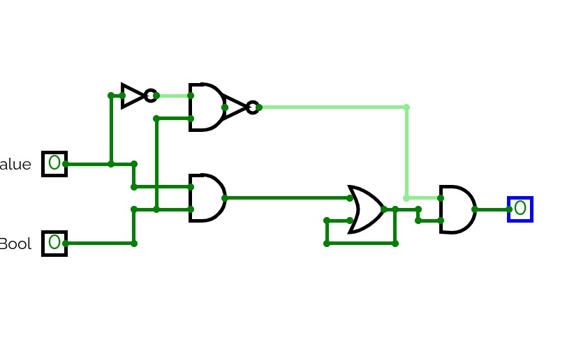
T Flip FlopExperiment No 9 d: Implementation of flip flops: SR, JK, D and T
Done by:
Saranga K. Mahanta
Sch Id: 18-14-038
D Flip Flop
D Flip FlopExperiment No. 9 c: Implementation of flip flops: D flip flop.
Done by:
Saranga K. Mahanta
Scholar Id: 18-14-038
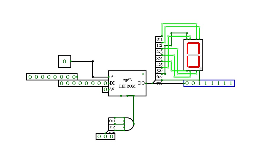
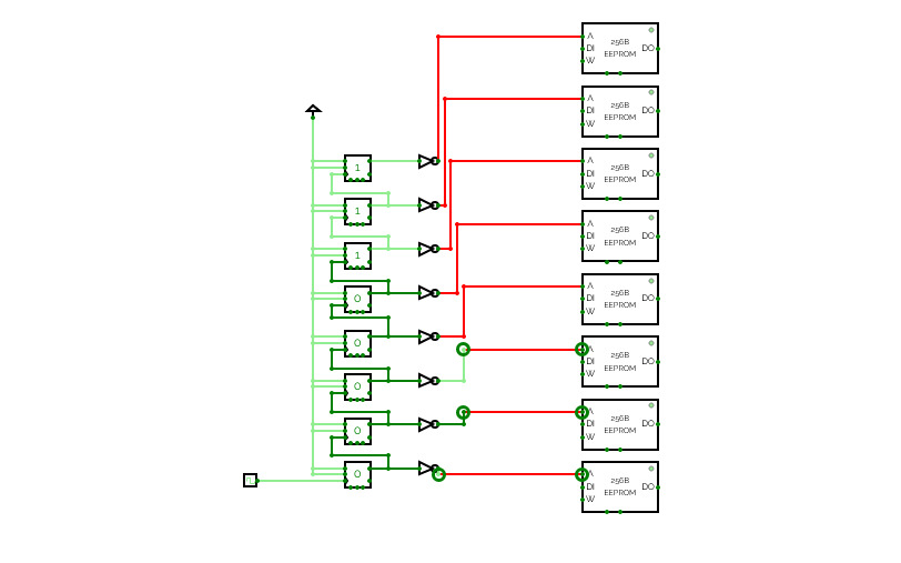
combinational logic with eeprom
combinational logic with eepromI'm using an EEPROM to replace combinational logic. The address is the decimal number in binary (or the counter). The data out is the 7-seg display (the leftmost bit is the decimal point).
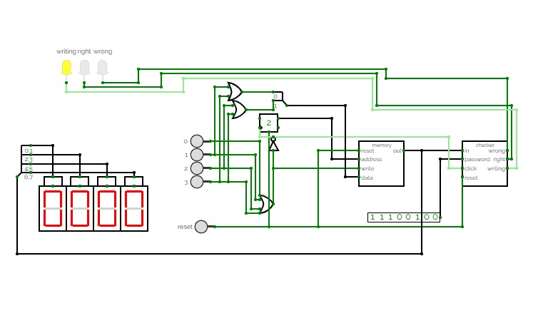
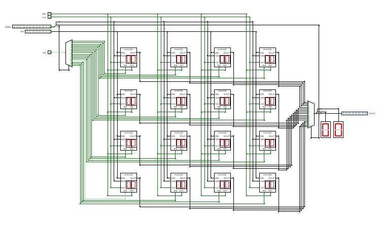
memory address
memory addresscircuit to allow a memory element to become a programmable controller


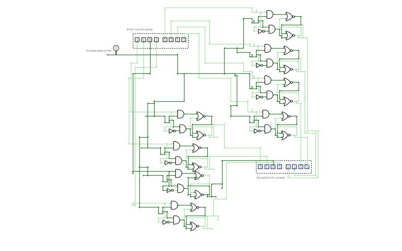
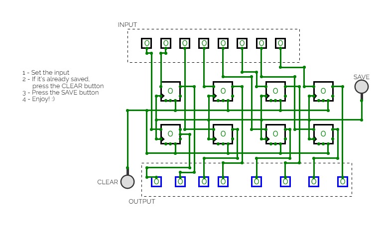
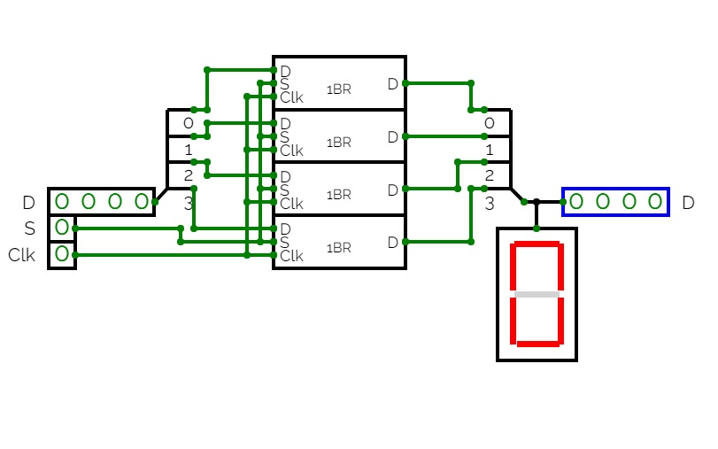
8 bit D-latch
8 bit D-latchThis is a version of a register, a part of a computer's Random Access Memory (RAM). It is capable of storing an 8-bit binary number. On the top left of the chip, you can set a binary number to be stored. Then to replace the old number, you must press the 'Enable data-write' switch to upload and store the new number.
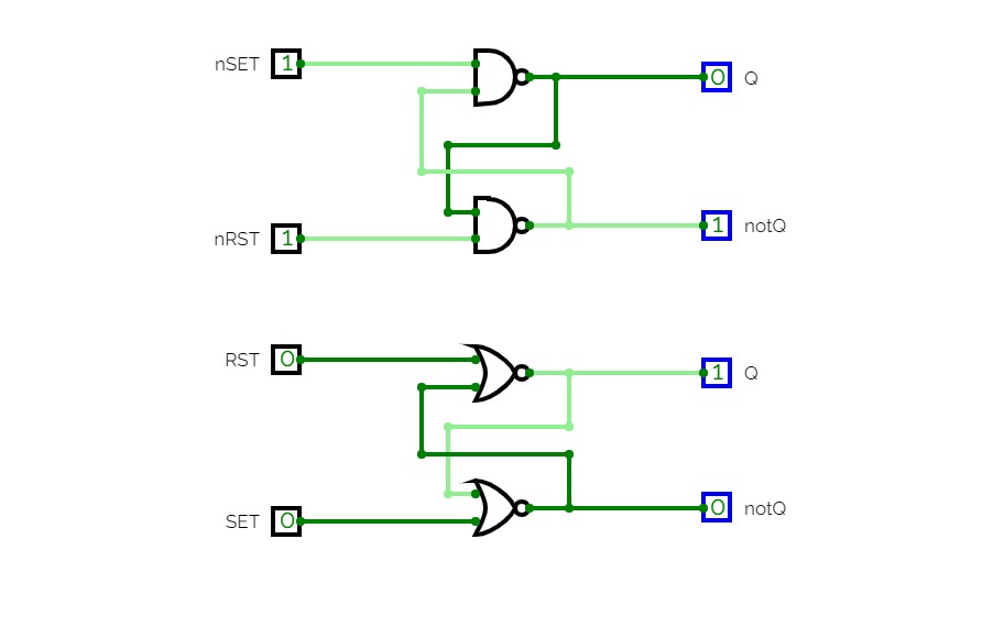

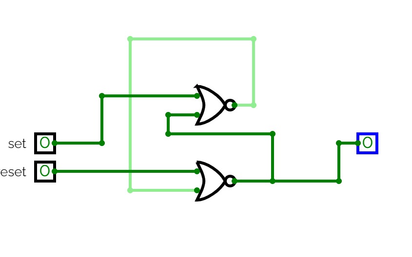
RS-trigger
RS-triggerTest asynchronous RS latch equvalent logic scheme
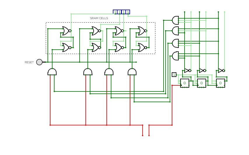
Static serial RAM with serial input
Static serial RAM with serial inputin this project i made a 4 bit RAM which can be written through serial communication(SCL - clock and SDA- data(1 or 0)) then a rising edge of a square wave is detected in the SCL pin, the enable pin of the SRAM cells are enabled in an order according to each clock pulse. simultaneously a data is given through the SDA pin according to the Nth clock pulse to the Nth SRAM cell.


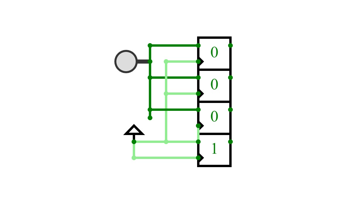
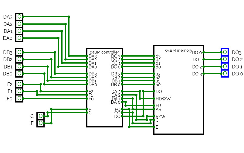
Project2
Project2Practice for utilizing ROM to produce an output based on some sequential input.


