

8bit Substractor
8bit Substractor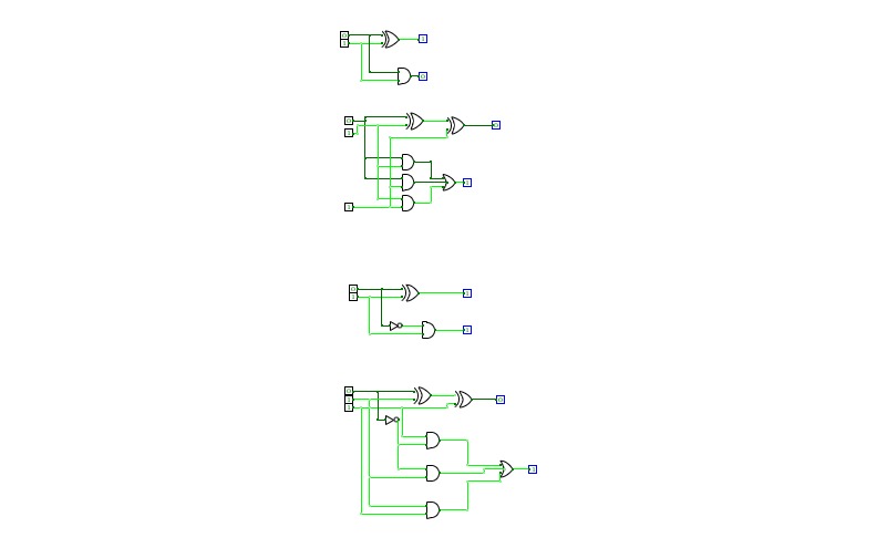
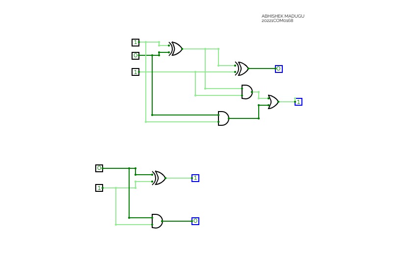
Half Adder ,Full adder , Half Subtractor and Full Subtractor
Half Adder ,Full adder , Half Subtractor and Full Subtractor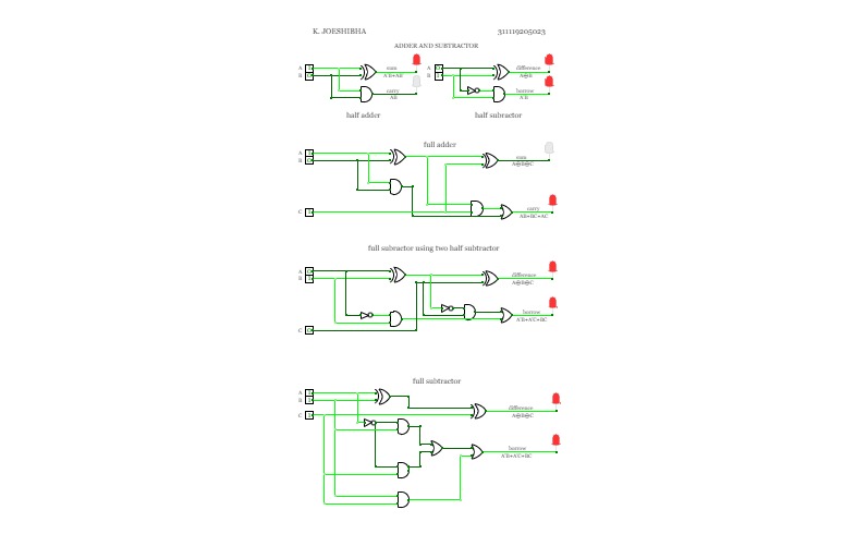
JOESHIBHA_ASS3
JOESHIBHA_ASS3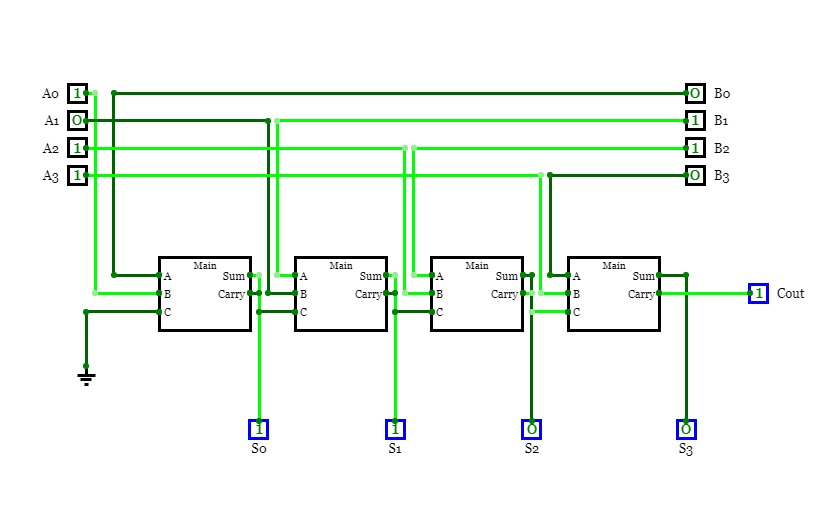
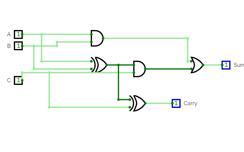
full Adder
full AdderFull Adder
Adders
Adders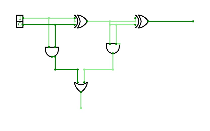
Untitled
Untitled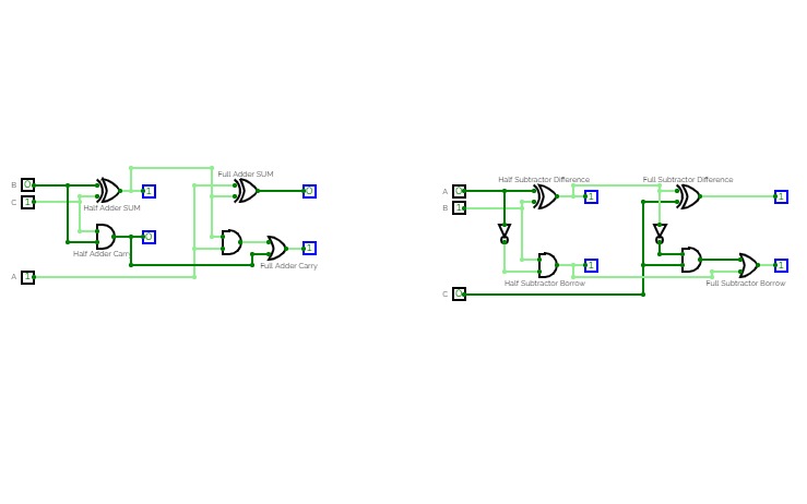

Adder and Subtractor
Adder and Subtractor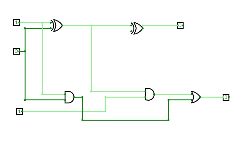
Full adder
Full adder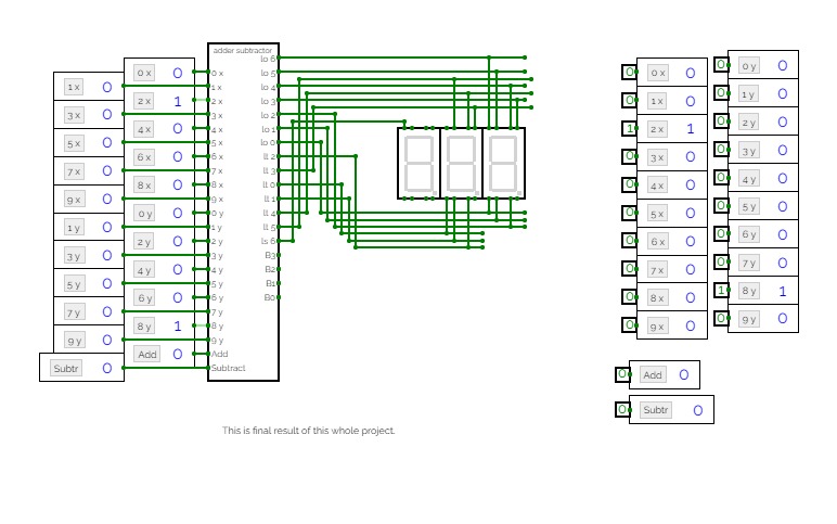

adder and subtractor
adder and subtractorThis is just a simple Full Adder and also a 4-bit simplistic magnitude comparator
Full adder
Full adder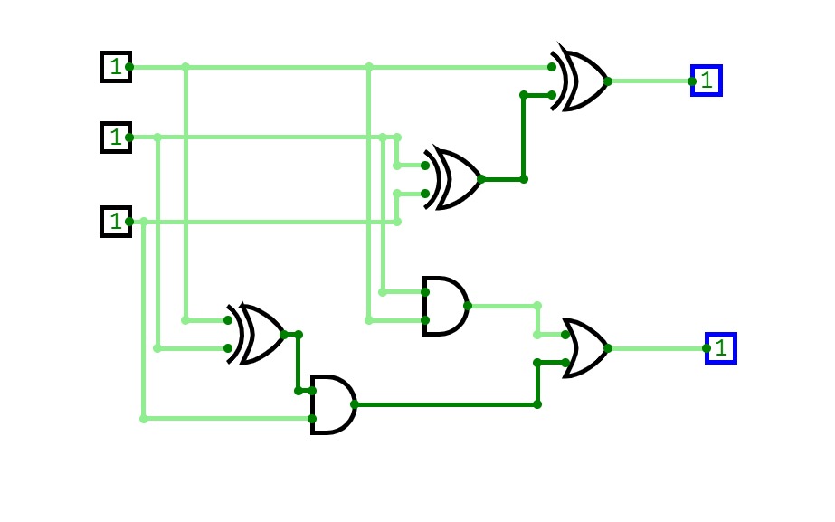
Untitled
Untitled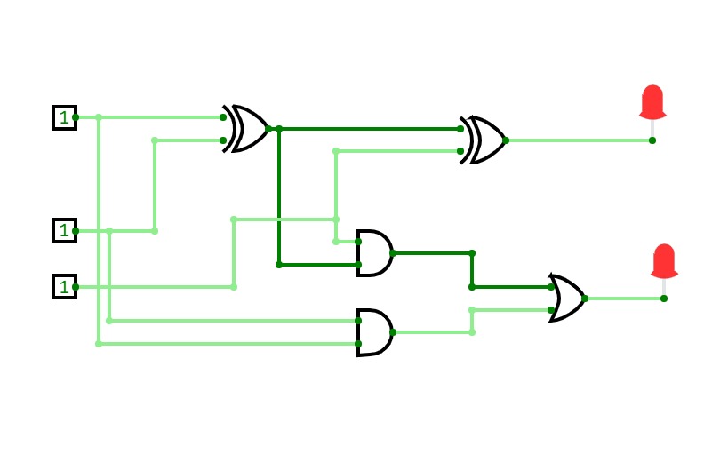
Full adder
Full adderThis is an full adder circuit
Combinational Logic Circuits
Combinational Logic CircuitsXOR, Half adder, Full adder, Multi-bit full adder, Comparator, Multi-bit comparator, Shifter, Multiplexer 4-to-1, Demultiplexer 1-to-4, Decoder 2-to4, ALU-Arthmetic Logic Unit

ADDER
ADDER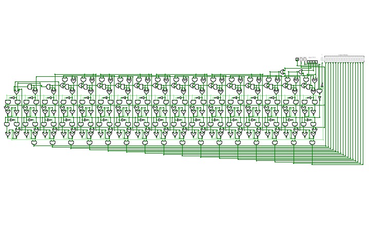

Serial BCD to binary
Serial BCD to binaryHello,
I have designed a special converter. Converts a BCD or Binary Coded Decimal number to 16-bit binary logical number. The special feature is the surprising sequential entry of numbers!
This conversion method uses a small number of logic gates and the operation is cyclical, so a clock is essential. Each BCD value entry is equal to one cycle. The converter consists of a register called the Accumulator, a 16-bit full adder and a wire connection that correctly multiplies the number by 10. A small control unit is also needed to monitor the system.
An Accumulator is a type of register, usually the first one used to store results.
The device works by adding a value from 0 to 9 to each BCD input, storing it in a register and then multiplying by 10. The cycle is repeated for each entry. so, for example, the number 123 in the BCD value 0001 0010 0011 is sent sequentially to the converter. The first number sent will be 0001. The adder will add 0001, then store the value in a register and multiply it by 10 in the binary form 1010, and the result will be 1010. We will then send a second BCD number 0010. This number will be added to the previous stored number 1010 and the resulting number will be 1100. This number is again stored in the register and multiplied by 10 according to the current time, the result will be 1111000. Then send a third BCD value 0011, which is added to the stored value 1111000 to get 1111011. Now read our final result 1111011!
This converter design is quick and easy. Unlike the others, it converts sequential BCD input values and contains a small number of logic gates. Dabble Double algorithms exist for this conversion, but they behave differently.
I have attached a diagram of how the device works below. I hope it will help you with your planning!
INSTRUCTIONS:
1. Reset the device before use!
(RST = Reset button)
2. Enter the BCD value!
(Inpu BCD)
3. After each entry, send the value!
(SND = Send)
4. Each entry is equal to one tick of the clock!
(CLK = Clock)
5. The error will be logged!
(E = Error)
6. Read the binary number!
(Output binary)
If you like my project, please give me a star (the button is on the bottom right), because it means a lot to me!
I hope you like the plan. I hope you enjoy the experience.

lab2
lab2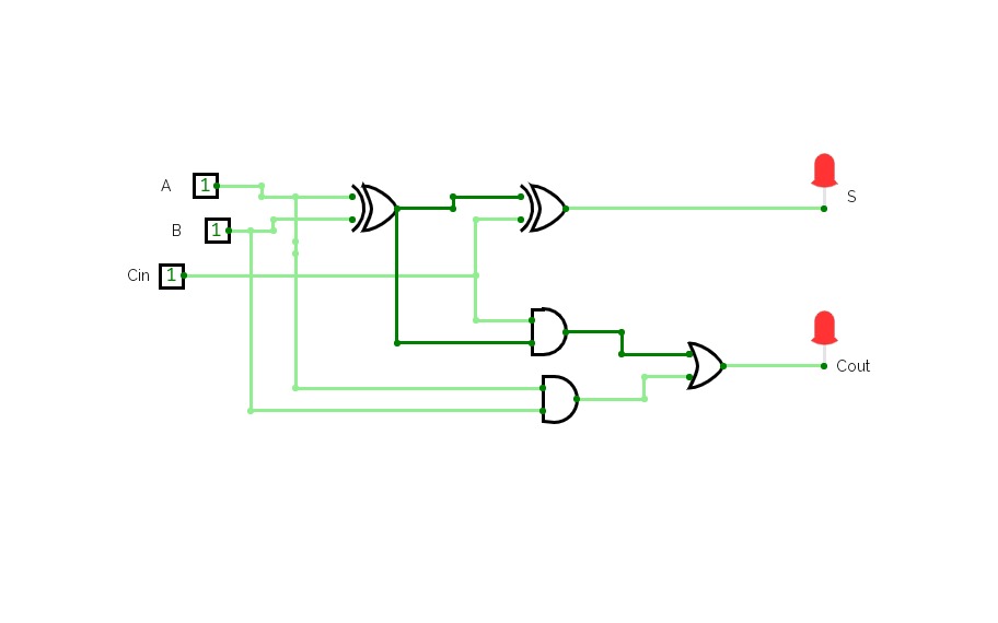

Experiment 4
Experiment 4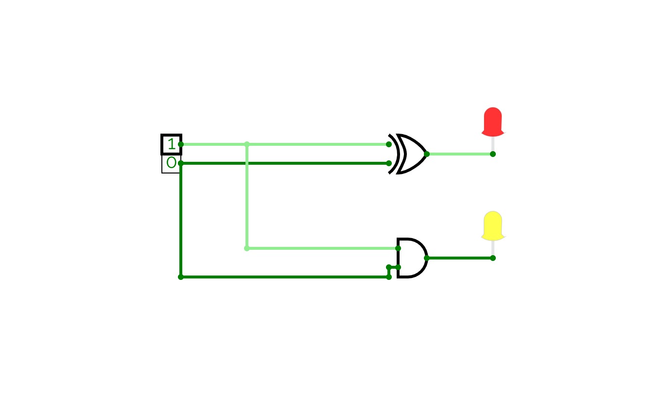
Experiment 4
Experiment 4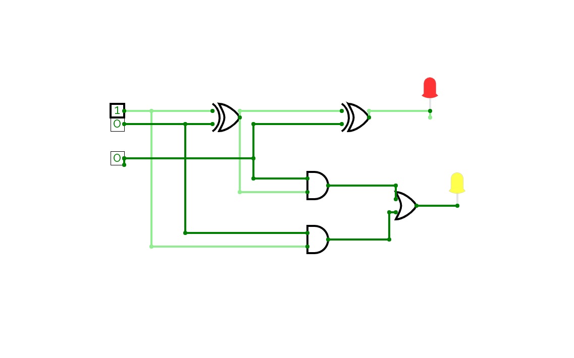
Experiment 4
Experiment 4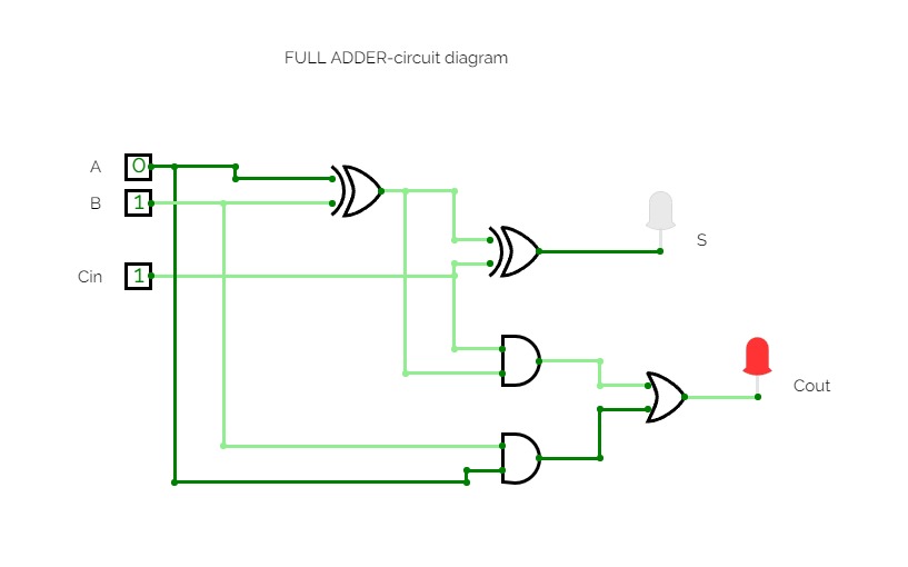

Experiment-4
Experiment-4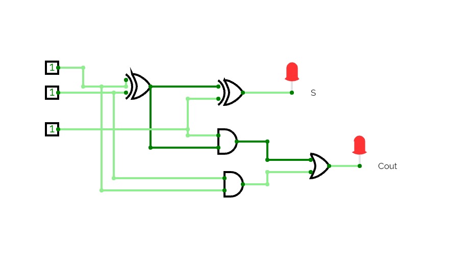

Experiment 4
Experiment 4
Experiment 4
Experiment 4
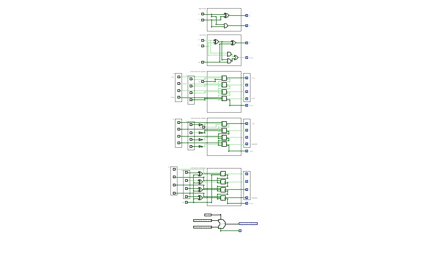
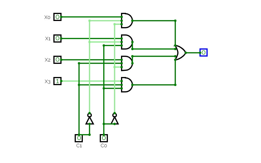
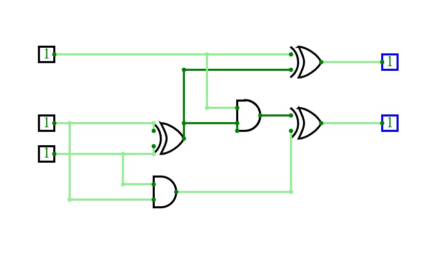
ALU_3Bits
ALU_3BitsThis is a replication of an ALU (Arithmetic and Logical Unit) containing a Full Adder, logical gates to invert both inputs separately, to make both inputs zero separately, to invert the output, to add both inputs or to get the logical result of AND (X, Y).
Instructions on how to use:
Double click on the main 3 bit inputs to set their value individually. Beware that any input of less or more than 3 bits will make the ALU malfunction. Also only input binary values. Inputs are signed in the 'Two's complement' method.
Click once on the control values to set them alternatively on '0' or '1'.
Outputs are read-only.
Values:
Input values are X and Y. They are 3 bits inputs.
Control values are ZX, NX, ZY, NY, F and NO. They are 1 bit inputs.
ZX = 1 means X input is '000', otherwise it is simply X.
NX = 1 means X input gets inverted (NOT(X)), otherwise it is simply X. This inverter happens after X has (or not) been set to zero.
ZY = 1 means Y input is '000', otherwise it is simply Y.
NX = 1 means Y input gets inverted (NOT(Y)), otherwise it is simply Y. This inverter happens after Y has (or not) been set to zero.
F = 1 means the full adder is selected for the ouput, otherwise the AND (X, Y) method is selected.
NO = 1 means the ouput will be inverted (NOT(OUT)), otherwise it is simply OUT. This happens after either the full adder or the AND logical gate.
Used gates are NOT, AND, OR, MUX.
Ouput is in three bits.
Flag outputs are ZR and NG.
ZR = 1 means the output is '000', otherwise it is any other combination of 3 bits
NG = 1 means the output is negative ('1xx'), otherwise it is positive ('0xx').
A light green line means the value it carries is '1', dark green means '0'.
Intermediate carries of added bits have been output in the circuit for a better understanding of how it works and are labeled R0, R1, R2 and R3
Possible circuits are:
ADD(X, Y)
ADD(NOT(X), Y)
ADD(X, NOT(Y))
ADD(NOT(X), NOT(Y))
ADD(0, Y)
ADD(X, 0)
ADD(0, 0)
ADD(NOT(0), Y)
ADD(NOT(X), 0)
ADD(NOT(0), 0)
ADD(0, NOT(Y))
ADD(X, NOT(0))
ADD(0, NOT(0))
ADD(NOT(0), NOT(Y))
ADD(NOT(X), NOT(0))
ADD(NOT(0), NOT(0))
AND(X, Y)
AND(NOT(X), Y)
AND(X, NOT(Y))
AND(NOT(X), NOT(Y))
AND(NOT(0), Y)
AND(NOT(X), 0)
AND(NOT(0), 0)
AND(0, NOT(Y))
AND(X, NOT(0))
AND(0, NOT(0))
AND(NOT(0), NOT(Y))
AND(NOT(X), NOT(0))
AND(NOT(0), NOT(0))
NOT(ADD(X, Y))
NOT(ADD(NOT(X), Y))
NOT(ADD(X, NOT(Y)))
NOT(ADD(NOT(X), NOT(Y)))
NOT(ADD(0, Y))
NOT(ADD(X, 0))
NOT(ADD(0, 0))
NOT(ADD(NOT(0), Y))
NOT(ADD(NOT(X), 0))
NOT(ADD(NOT(0), 0))
NOT(ADD(0, NOT(Y)))
NOT(ADD(X, NOT(0)))
NOT(ADD(0, NOT(0)))
NOT(ADD(NOT(0), NOT(Y)))
NOT(ADD(NOT(X), NOT(0)))
NOT(ADD(NOT(0), NOT(0)))
NOT(AND(X, Y))
NOT(AND(NOT(X), Y))
NOT(AND(X, NOT(Y)))
NOT(AND(NOT(X), NOT(Y)))
NOT(AND(NOT(0), Y))
NOT(AND(NOT(X), 0))
NOT(AND(NOT(0), 0))
NOT(AND(0, NOT(Y)))
NOT(AND(X, NOT(0)))
NOT(AND(0, NOT(0)))
NOT(AND(NOT(0), NOT(Y)))
NOT(AND(NOT(X), NOT(0)))
NOT(AND(NOT(0), NOT(0)))

Experiment-02: IMPLEMENTATION OF COMBINATIONAL CIRCUITS
Experiment-02: IMPLEMENTATION OF COMBINATIONAL CIRCUITShello these are adder circuits

Lab- 2
Lab- 2Airthmatic addition of 2 & 3 bits

Akmal Dzaki Rahmatullah_24060124140151_A1
Akmal Dzaki Rahmatullah_24060124140151_A1
Two bit adder
Two bit adderThe half adder and full adder modules are built using verilog. These modules are then combined to form a two bit adder.


