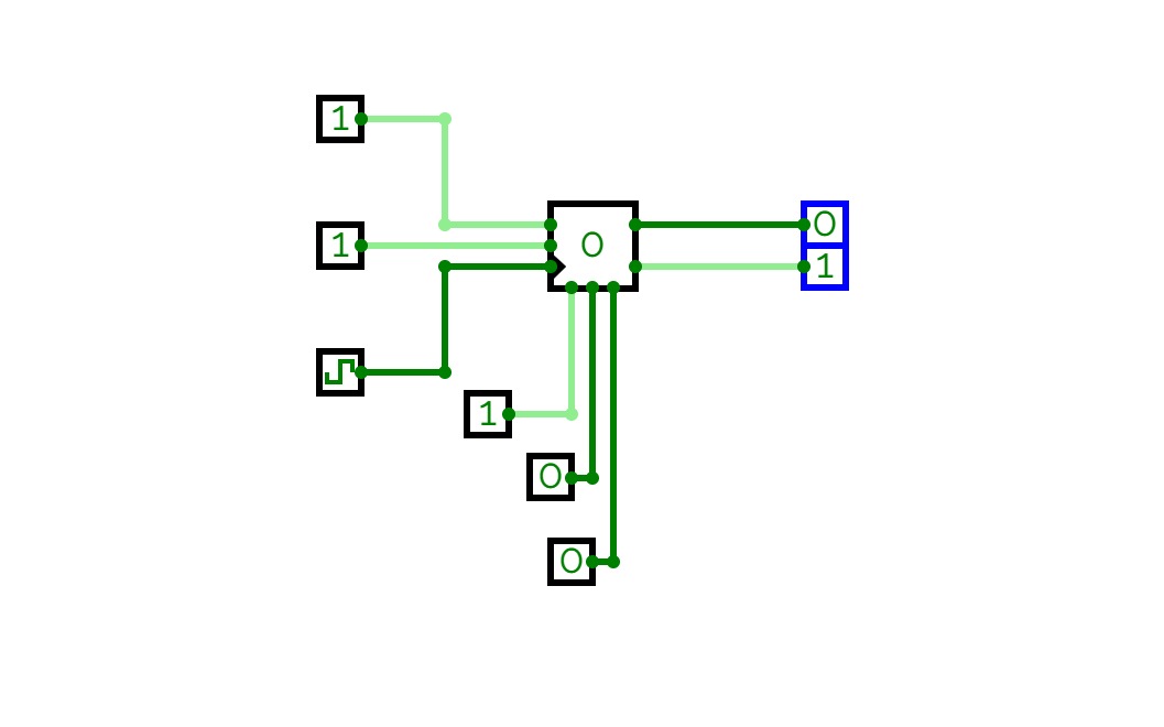

JK Flip-Flop using Sequential Logic
JK Flip-Flop using Sequential Logic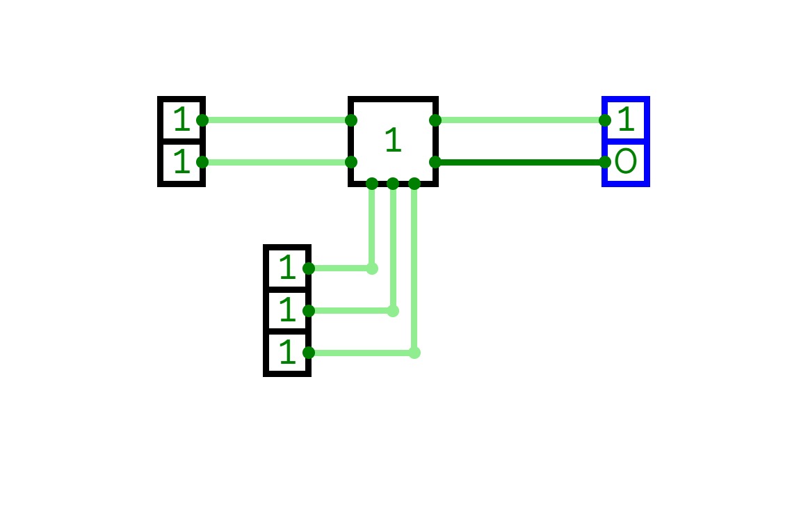
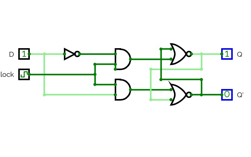
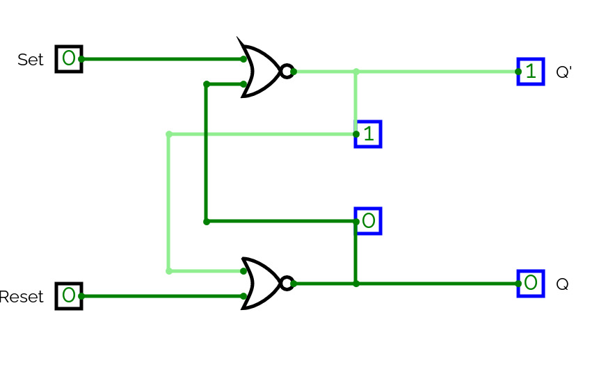
SR Flip-Flop using Sequential Logic
SR Flip-Flop using Sequential Logic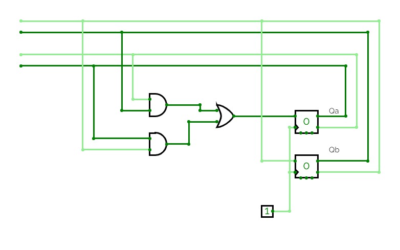
UpCounter_2Bit
UpCounter_2BitI built a 2 bit up counter without any enable. I am manually controlling the clock

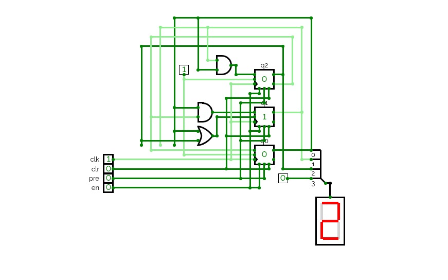
BCD-counter
BCD-counter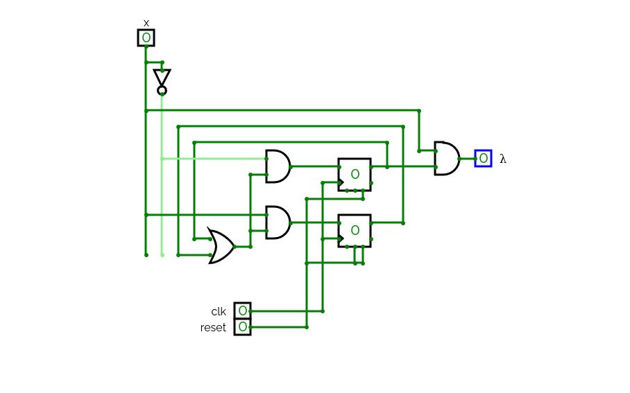
sequence detector
sequence detectorMoore and Mealy machines detection the binary sequence 01.
Encoding states: one-hot.
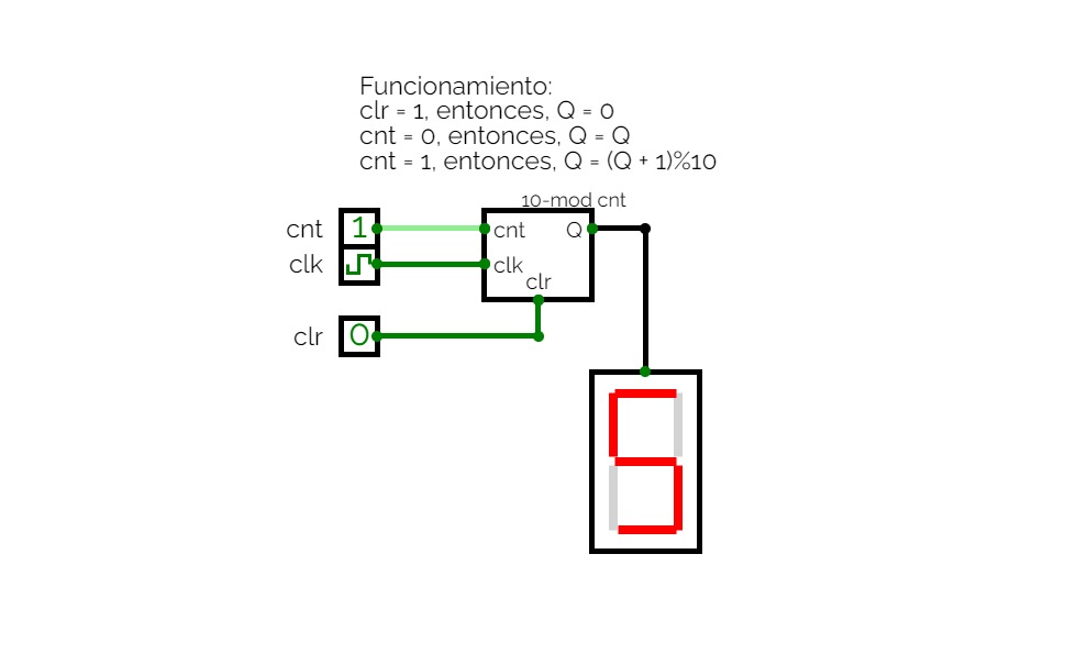
5-mod counter
5-mod counter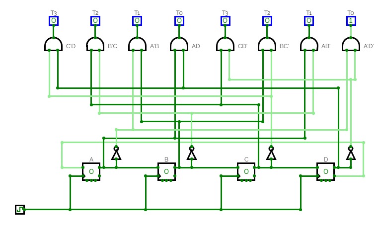

[CSCA] Counters and Timing Signals
[CSCA] Counters and Timing SignalsCounters and timing signal generators discussed in the Computer Science and Computer Architectures [CSCA] course at the University of Applied Sciences CAMPUS 02, Graz, Austria.
The project features the following circuits:
-
Sample 2-Bit Counter - a simple counter exploratory developed by students during the lectures.
- Sample 2-Bit Counter with Timing Signals - that simple counter extended with decoder to provide timing signals.
- 2-Bit Switch-Tail Ring Counter - developed by using D flip-flops.
- 2-Bit Johnson Counter - developed by extending the 2-Bit Switch-Tail Ring Counter with decoder to provide timing signals.
- 4-Bit Switch-Tail Ring Counter - developed by extending the 2-Bit Switch-Tail Ring Counter with two more D flip-flops. [learn more (see chapters at the bottom of the page)]
- 4-Bit Johnson Counter - developed by extending the 4-Bit Switch-Tail Ring Counter with decoder to provide timing signals. [learn more (see chapters at the bottom of the page)]
[CSCA] Registers and Memory
[CSCA] Registers and MemoryRegisters and memory elements discussed in the Computer Science and Computer Architectures [CSCA] course at the University of Applied Sciences CAMPUS 02, Graz, Austria.
The project features the following circuits:
- 4-Bit Register - developed by using D flip-flops.
- 4-Bit Register (Enabling the Clock Signal) - 4-Bit Register with enabling of the register implemented via enabling of the clock signal.
- 4x4-Bit Memory - with read and write access and reading buffer set to zeros in case of writing.
- Tri-State Buffers - explains the tri-state buffer element.
-
Mutually Exclusive Tri-State Buffers - demonstrates how to use tri-state buffers to mutually exclude parts of a circuit.
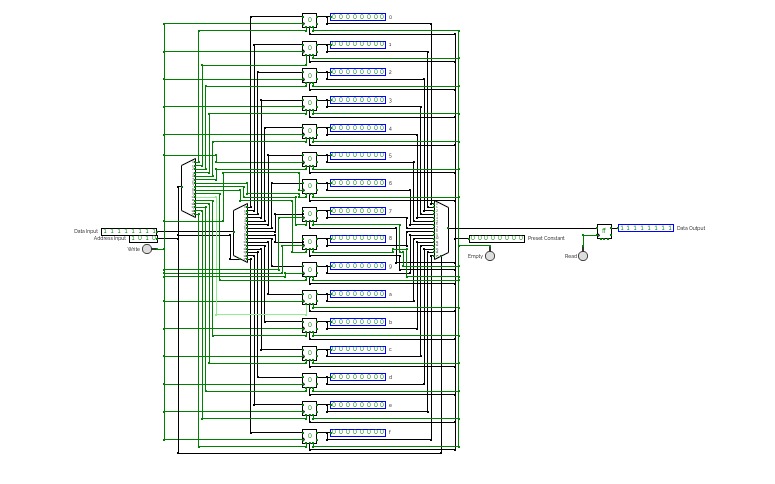
- 4x4-Bit Memory with Tri-State Buffers - developed by extending the 4x4-Bit Memory with Tri-state buffers to cut of the reading buffer in case of writing.
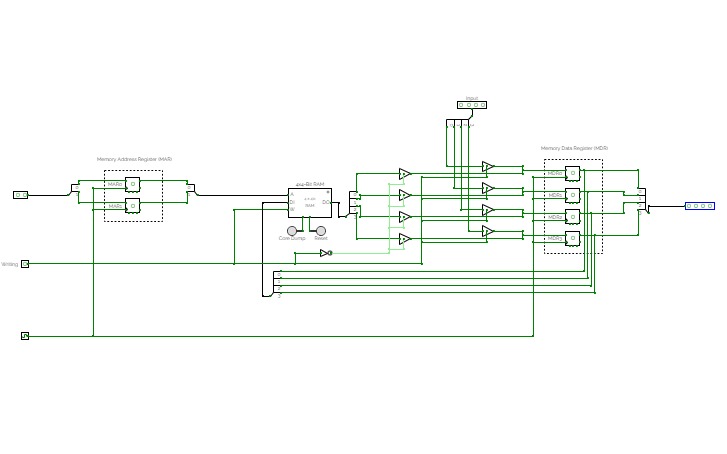
- 4x4-Bit Memory with MAR and MDR - developed by extending the 4x4-Bit Memory with Tri-State Buffers with the Memory Address Register (MAR) and Memory Data Register (MDR).
- 4x4-Bit Random Access Memory (RAM) - demonstrates using the built-in RAM element.
-
4x4-Bit Random Access Memory (RAM) with MAR and MDR - demonstrates using the built-in RAM element extended with the Memory Address Register (MAR) and Memory Data Register (MDR).
[CSCA] Latches and Flip-flops
[CSCA] Latches and Flip-flops
Latches and flip-flops as discussed in the Computer Science and Computer Architectures [CSCA] course at the University of Applied Sciences CAMPUS 02, Graz, Austria.
The project features the following circuits:
- SR Latch - demonstrates the behavior of an SR Latch. [learn more]
-
Clock - demonstrates the Clock Signal. [learn more]
- Clocked SR Latch - developed by bringing the Clock Signal to the SR Latch. [learn more]
- D Latch - demonstrates the behavior of a D Latch. [learn more]
- Clocked D Latch - developed by bringing the Clock Signal to the D Latch. [learn more]