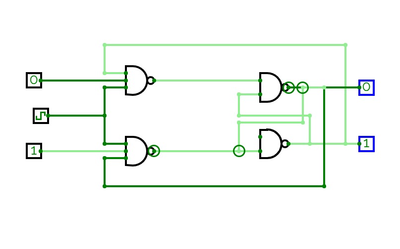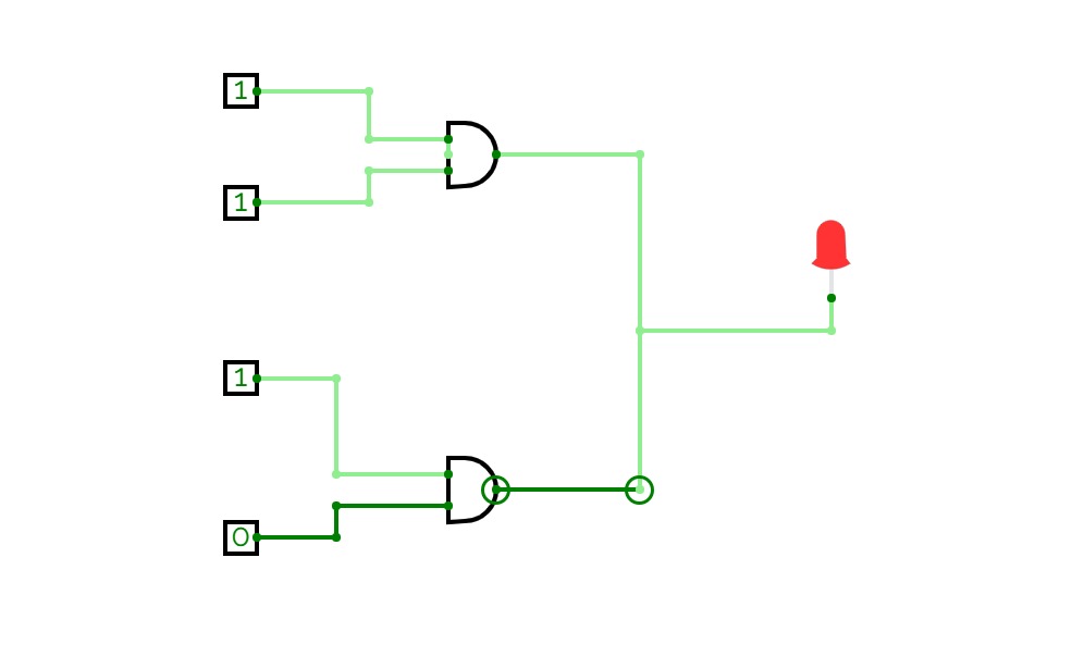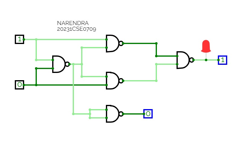

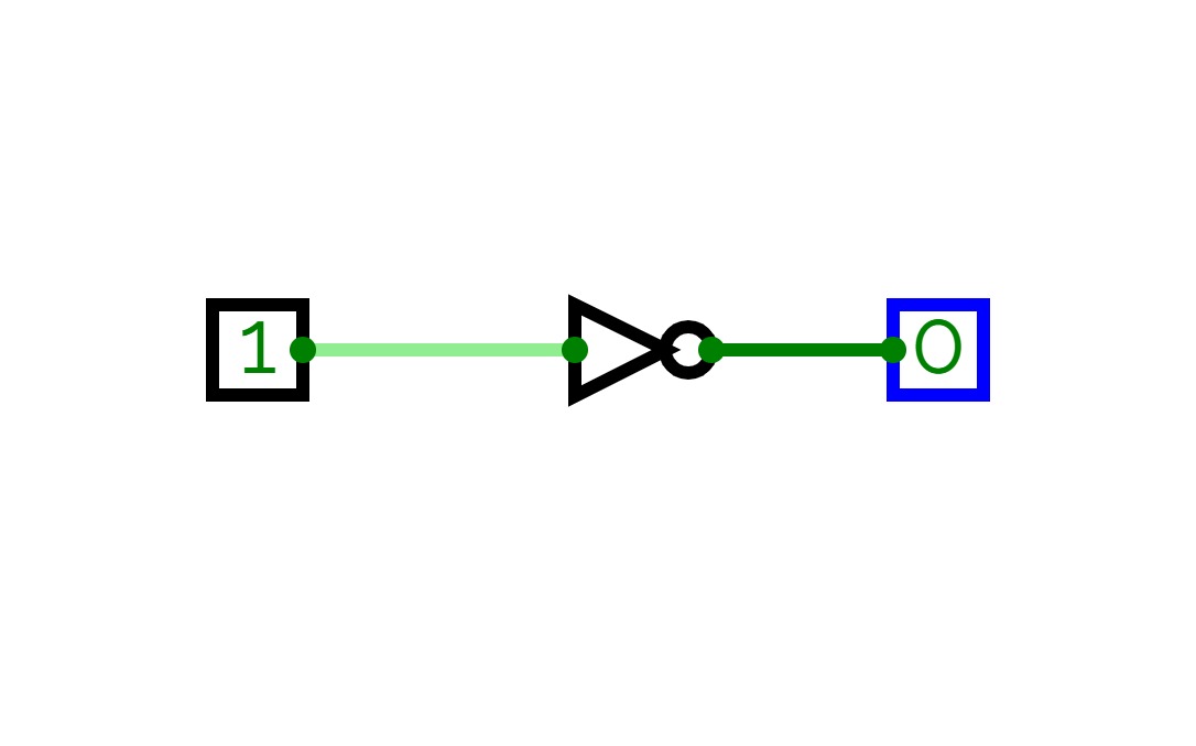

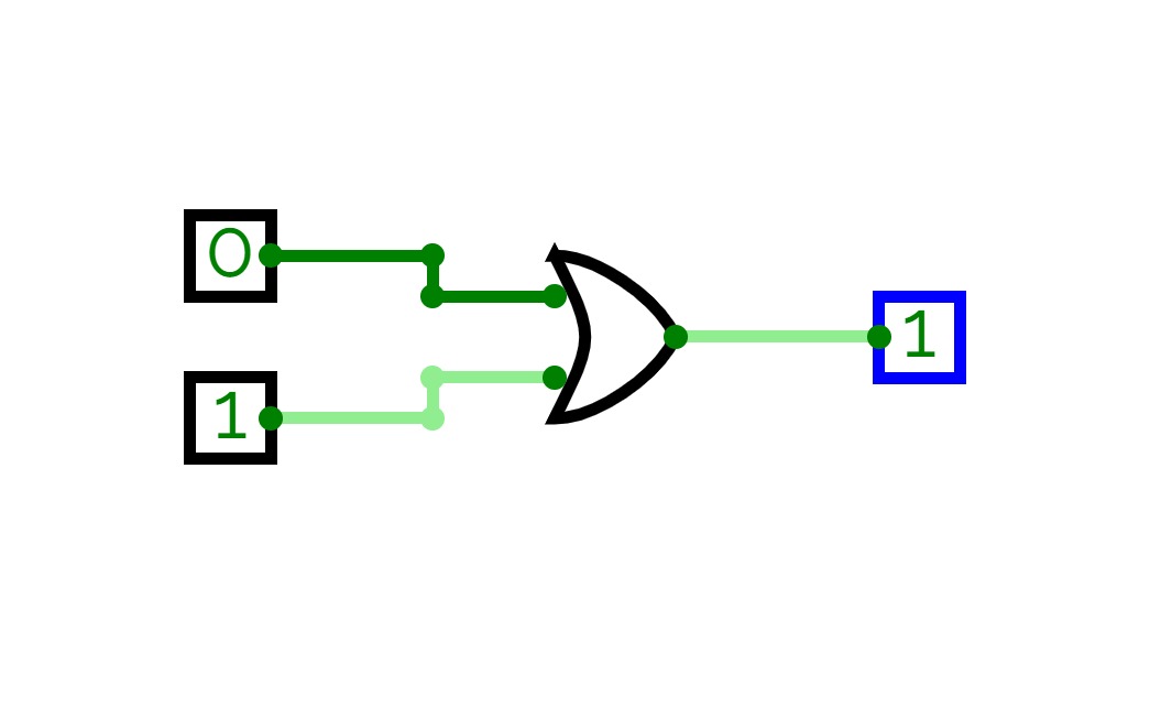
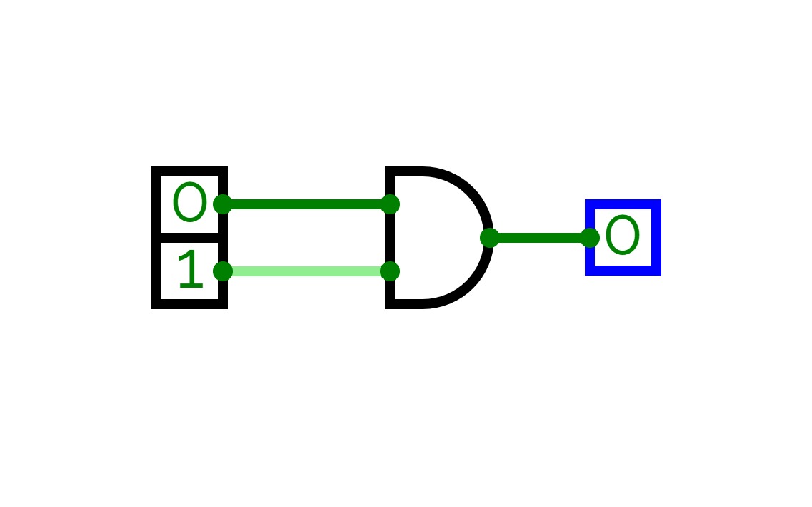
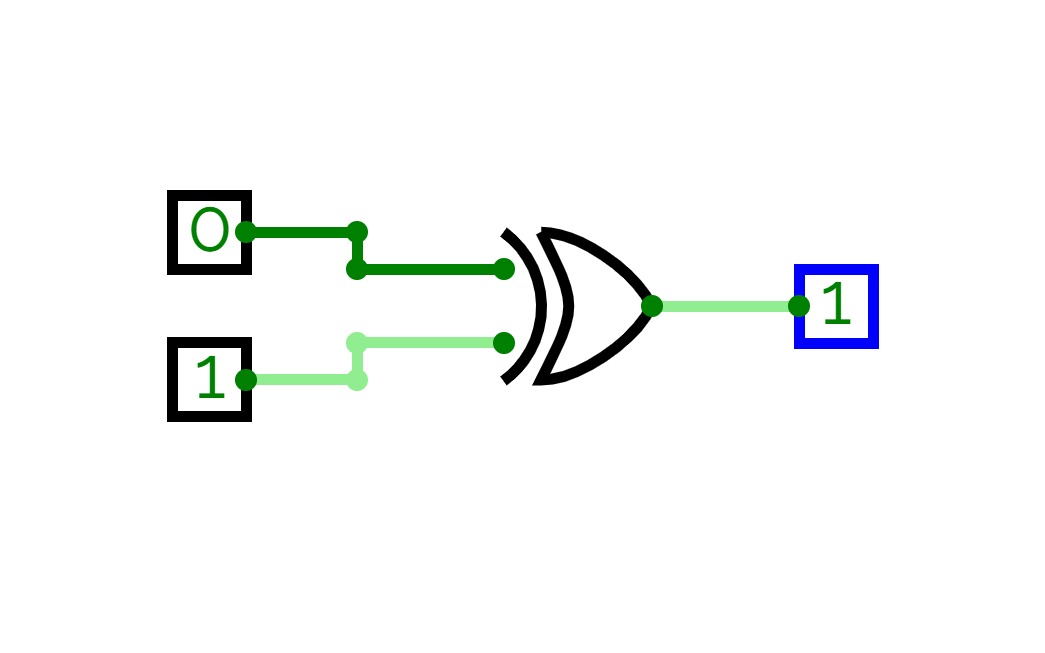
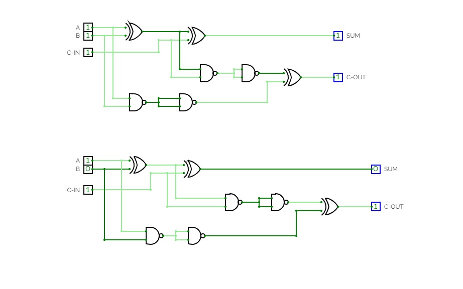
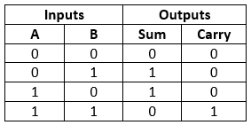
Full Adder is the adder that adds three inputs and produces two outputs. The first two inputs are A and B and the third input is an input carry as C-IN. The output carry is designated as C-OUT and the normal output is designated as S which is SUM. A full adder logic is designed in such a manner that can take eight inputs together to create a byte-wide adder and cascade the carry bit from one adder to another. we use a full adder because when a carry-in bit is available, another 1-bit adder must be used since a 1-bit half-adder does not take a carry-in bit. A 1-bit full adder adds three operands and generates 2-bit results.
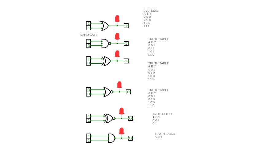
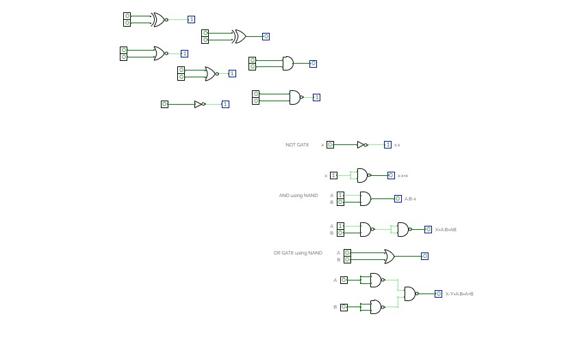
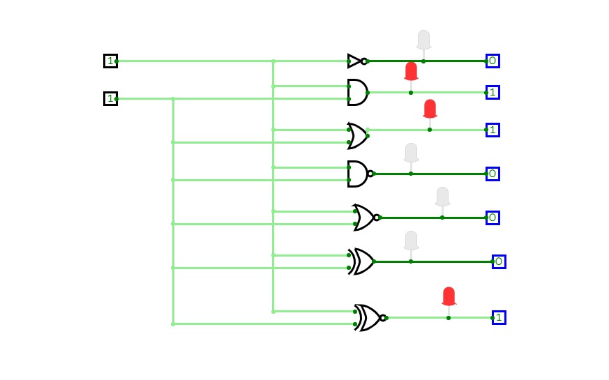
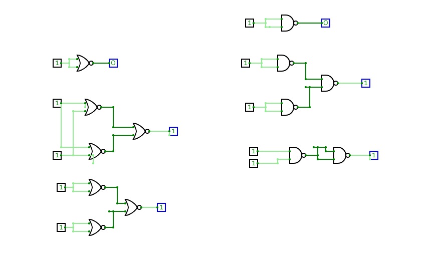
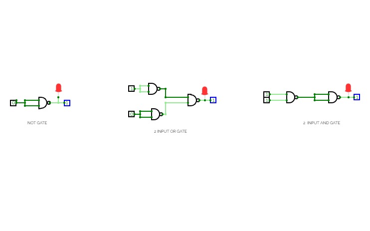
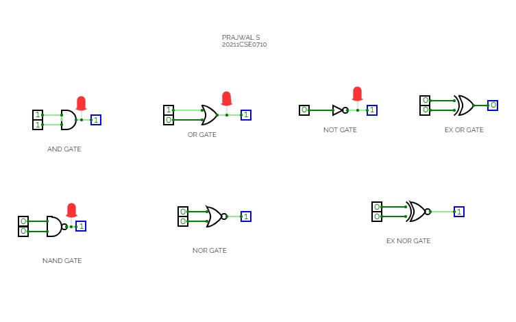
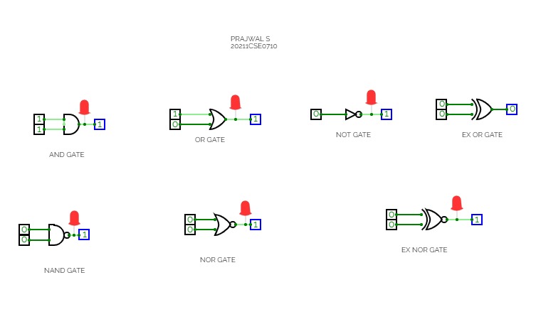
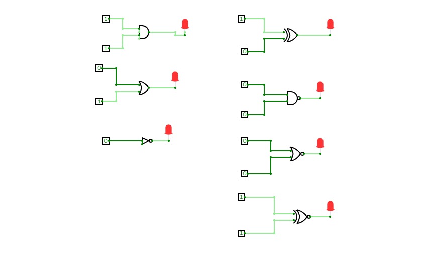
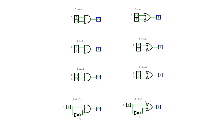
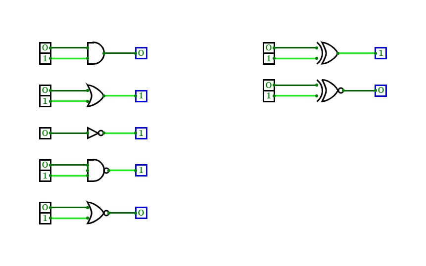
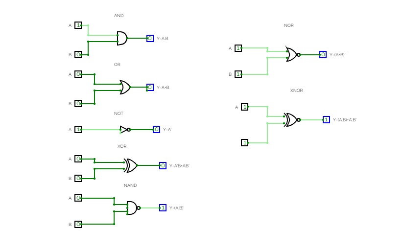
Here we need to make a full adder on simulator by using gate ie. XOR gate and NAND gate after that we need to check whether it is right or not by giving input 0 or 1 . As we have already make a truth table for it in order to check and match whether the circuit is connected or working properly well or not.
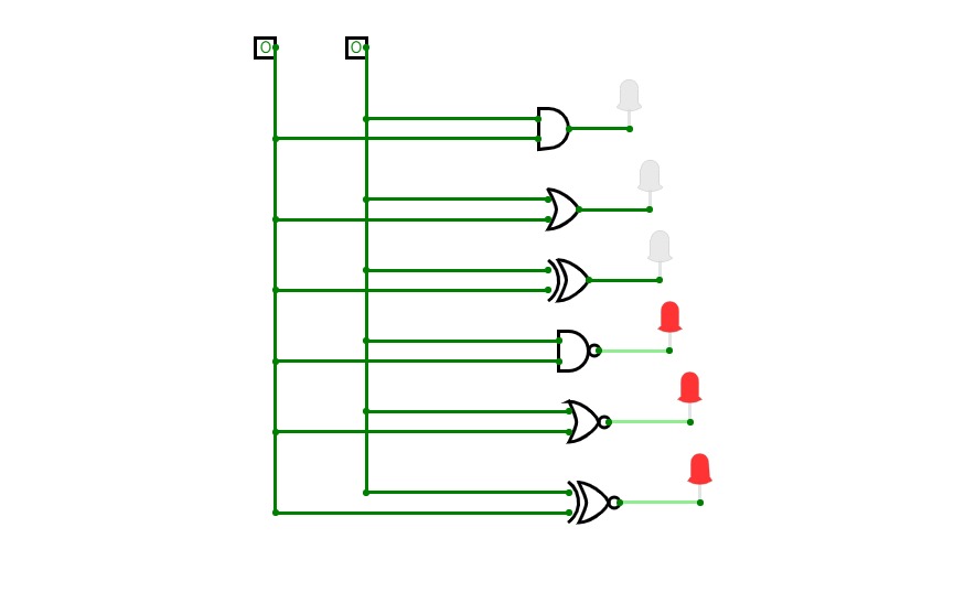
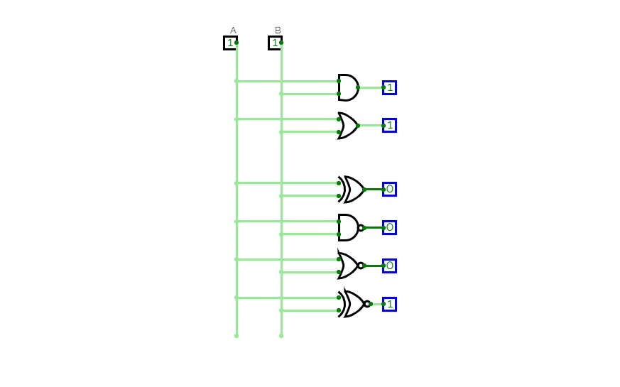
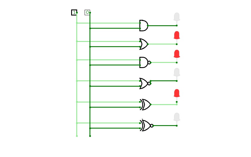
TRUTH TABLE
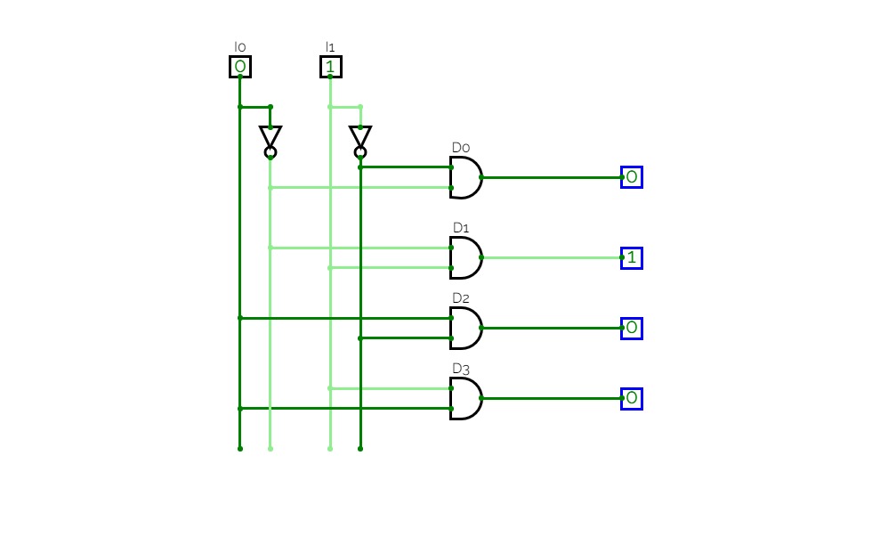
2*4 DECODER
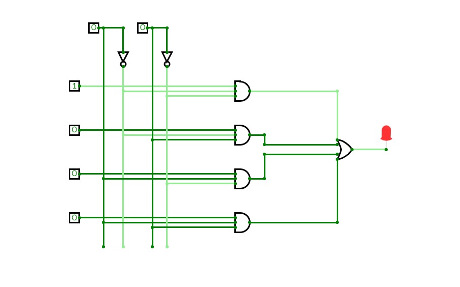
2*4 DECODERA decoder is a multiple input, multiple output logic circuit that changes codes i/ps into coded o/ps, where both the inputs and outputs are dissimilar for instance n-to-2n, and binary coded decimal decoders. Decoding is essential in applications like data multiplexing, memory address decoding, and 7 segment display. The best example of decoder circuit would be an AND-gate because when all its inputs are “High.”, the output of this gate is “High” which is called “active High output”. As an alternative to AND gate, the NAND gate is connected the output will be “Low” (0) only when all its inputs are “High”. Such o/p is called “active low output”.
2 to 4 Line Decoder
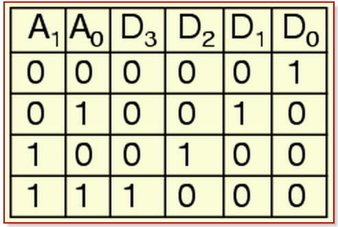
In this type of decoders, decoders have two inputs namely A0, A1, and four outputs denoted by D0, D1, D2, and D3. As you can see in the following truth table – for every input combination, one o/p line is turned on.D0 =A1 A0, ( minterm m0) which corresponds to input 00 D1 =A1 A0, ( minterm m1) which corresponds to input 01 D2 =A1 A0, ( minterm m2) which corresponds to input 10 D3 =A1 A0, ( minterm m3) which corresponds to input 11.
The circuit is implemented using AND gates. In this circuit, the logic equation for D0 is A1/A0, and so on. Thus, each output of the decoder will be generated to the input combination.
Truth Table
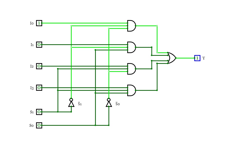
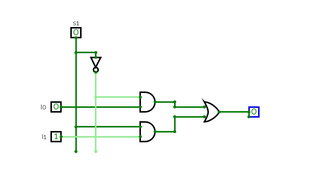
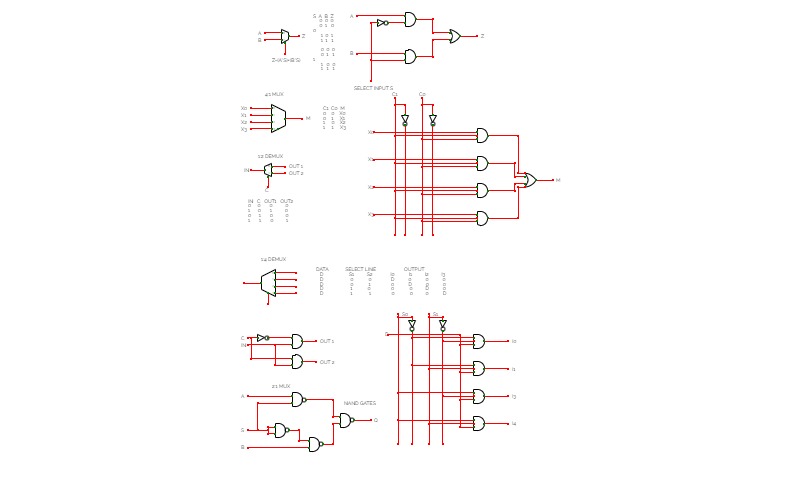
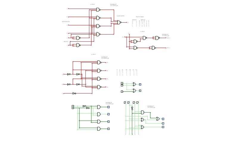
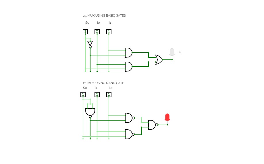
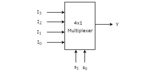
4x1 Multiplexer
4x1 MultiplexerMultiplexer is a combinational circuit that has maximum of 2n data inputs, ‘n’ selection lines and single output line. One of these data inputs will be connected to the output based on the values of selection lines.
Since there are ‘n’ selection lines, there will be 2n possible combinations of zeros and ones. So, each combination will select only one data input. Multiplexer is also called as Mux.
4x1 Multiplexer
4x1 Multiplexer has four data inputs I3, I2, I1 & I0, two selection lines s1 & s0 and one output Y. The block diagram of 4x1 Multiplexer is shown in the following figure.
One of these 4 inputs will be connected to the output based on the combination of inputs present at these two selection lines. Truth table of 4x1 Multiplexer is shown below.
TRUTH TABLE
Selection LinesOutputS1S0Y00I001I110I211I3
From Truth table, we can directly write the Boolean function for output, Y as
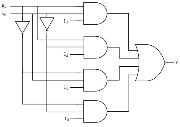
Y=S1′S0′I0+S1′S0I1+S1S0′I2+S1S0I3Y=S1′S0′I0+S1′S0I1+S1S0′I2+S1S0I3
We can implement this Boolean function using Inverters, AND gates & OR gate. The circuit diagram of 4x1 multiplexer is shown in the following figure.
CIRCUIT DAIGRAM
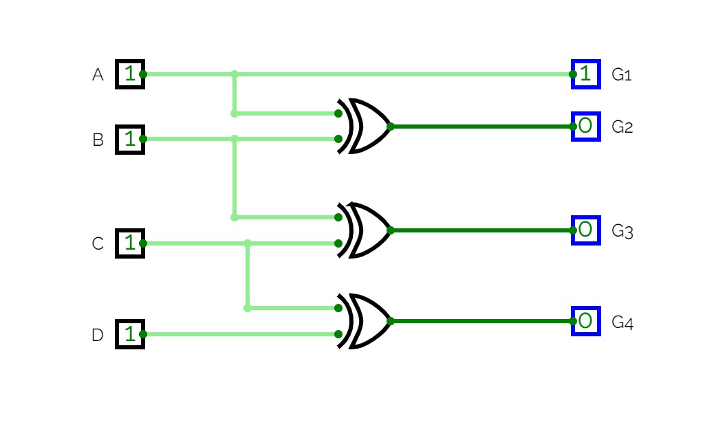
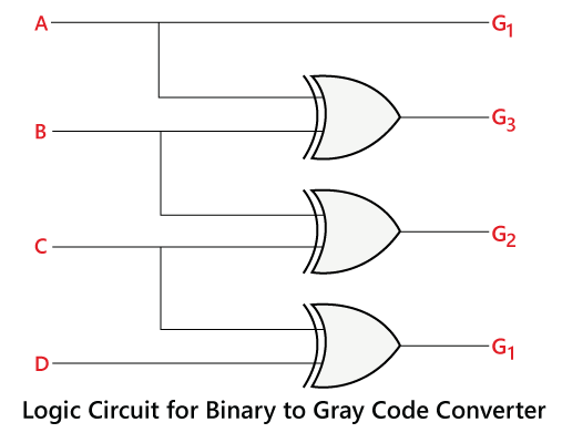
4 BIT BINARY TO GRAY CODE
4 BIT BINARY TO GRAY CODEBinary to Gray code conversion
The Binary to Gray code converter is a logical circuit that is used to convert the binary code into its equivalent Gray code. By putting the MSB of 1 below the axis and the MSB of 1 above the axis and reflecting the (n-1) bit code about an axis after 2n-1 rows, we can obtain the n-bit gray code.
In 4-bit gray code, the 3-bit code is reflected against the axis drawn after the 24-1-1th =8th row.
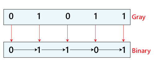
Just like Binary to Gray code conversion; it is also a very simple process. There are the following steps used to convert the Gray code into binary.
- Just like binary to gray, in gray to binary, the 1st bit of the binary number is similar to the MSB of the Gray code.
- The 2nd bit of the binary number is the same as the 1st bit of the binary number when the 2nd bit of the Gray code is 0; otherwise, the 2nd bit is altered bit of the 1st bit of binary number. It means if the 1st bit of the binary is 1, then the 2nd bit is 0, and if it is 0, then the 2nd bit be 1.
- The 2nd step continues for all the bits of the binary number.
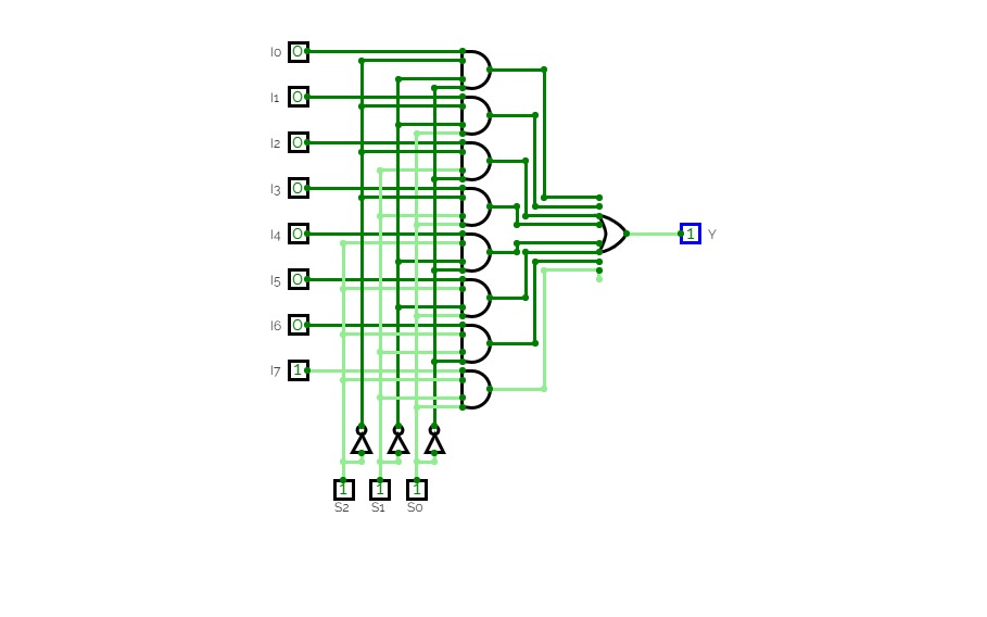
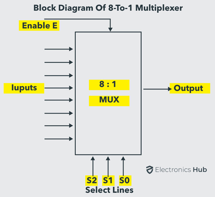
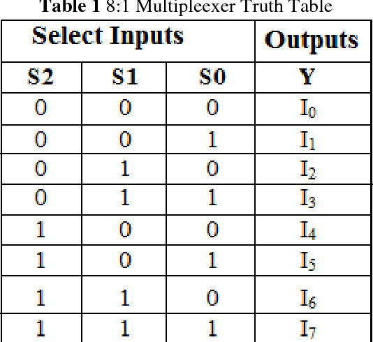
8x1 Multiplexer
8x1 Multiplexer8x1 Multiplexer
In the 8 to 1 multiplexer, there are total eight inputs, i.e., A0, A1, A2, A3, A4, A5, A6, and A7, 3 selection lines, i.e., S0, S1and S2 and single output, i.e., Y. On the basis of the combination of inputs that are present at the selection lines S0, S1, and S2, one of these 8 inputs are connected to the output.
Let the 8x1 Multiplexer has eight data inputs I7 to I0, three selection lines s2, s1 & s0 and one output Y. The Truth table of 8x1 Multiplexer is shown below.
BLOCK DIAGRAM