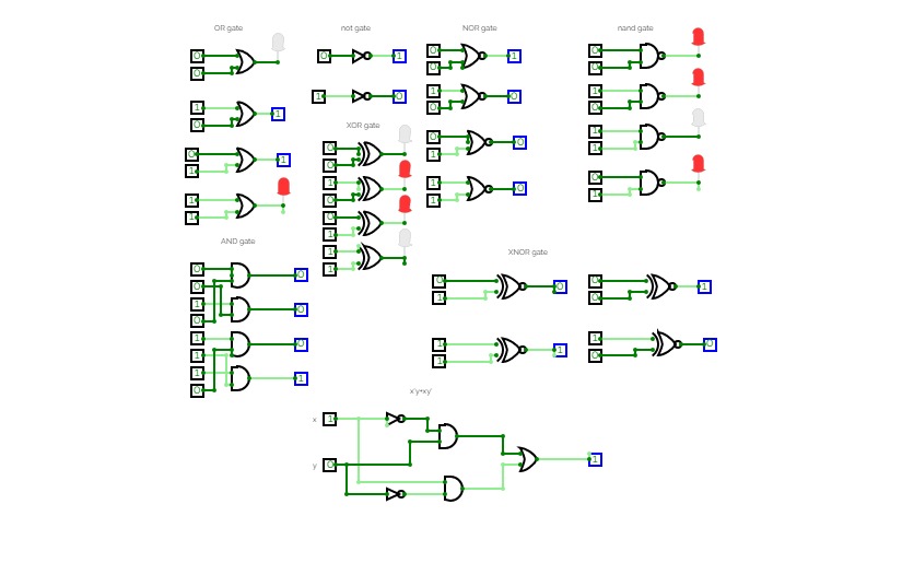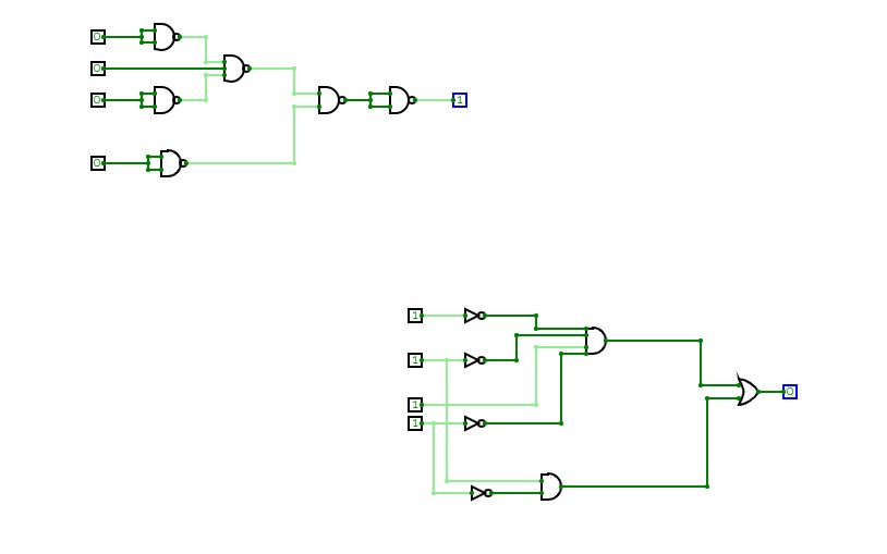

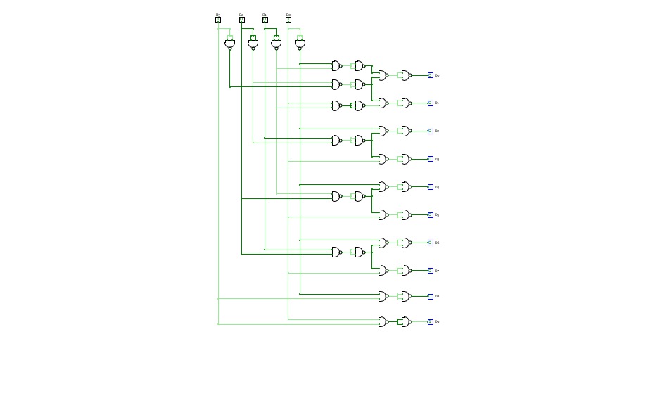
Decimal to Binary Encoder & Decoder
Decimal to Binary Encoder & Decoder
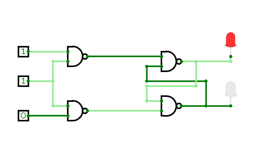

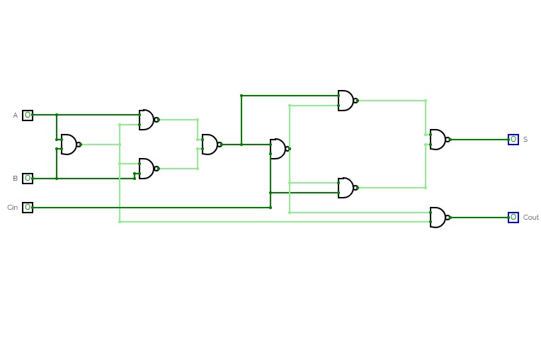
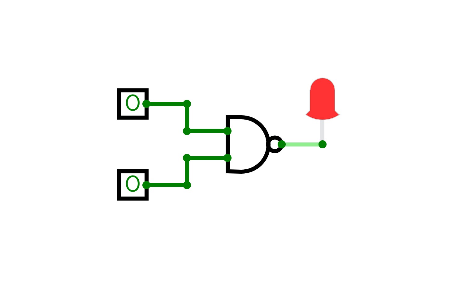
SR Flip Flop
SR Flip FlopThe basic NAND gate RS flip flop circuit is used to store the data and thus provides feedback from both of its outputs again back to its inputs. The RS flip flop actually has three inputs, SET, RESET and its current output Q relating to its current state.
Truth Table for RS flip –flop
Clk
R
S
Q
Q’
0
X
X
Previous or Memory State
1
1
0
0
1
1
0
1
1
0
1
0
0
Previous or Memory State
1
1
1
Invalid State
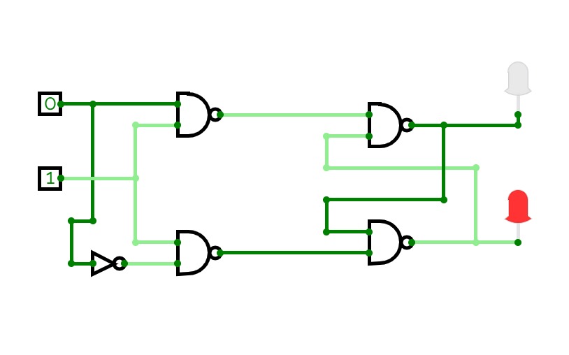
D flip-flop
D flip-flopA D flip flop has a single data input. This type of flip flop is obtained from the SR flip flop by connecting the R input through an inverter, and the S input is connected directly to data input. The modified clocked SR flip-flop is known as D-flip-flop and is shown below. From the truth table of SR flip-flop we see that the output of the SR flip-flop is in unpredictable state when the inputs are same and high. In many practical applications, these input conditions are not required. These input conditions can be avoided by making them complement of each other.
Truth Table for D flip-flop
Clk
D
Q
Q’
0
1
Previous or memory state
0
1
1
0
0
1
1
1
1
0
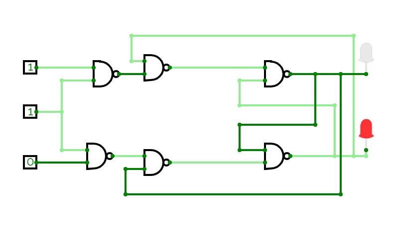
JK flip-flop
JK flip-flopIn a RS flip-flop the input R=S=1 leads to an indeterminate output. The RS flip-flop circuit may be re-joined if both inputs are 1 than also the outputs are complement of each other as shown in characteristics table below.
Truth Table for JK flip-flop
Input
Output
Clk
J
K
Q
Q’
0
X
X
Previous or Memory State
1
1
0
1
0
1
0
1
0
1
1
0
0
Previous or Memory State
1
1
1
Toggle State
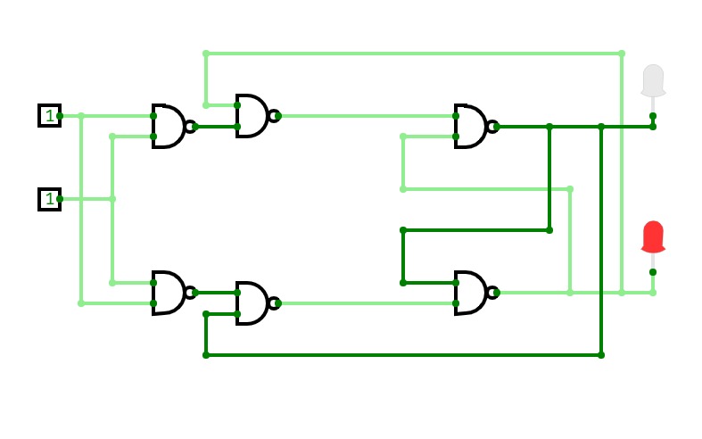
T flip-flop
T flip-flopT flip-flop is known as toggle flip-flop. The T flip-flop is modification of the J-K flip-flop. Both the JK inputs of the JK flip – flop are held at logic 1 and the clock signal continuous to change as shown in table below.
Truth Table of T flip-flop
Clk
T
Q
Q’
0
1
Previous or memory state
0
0
1
0
1
1
Toggle state