Flip Flop Verifications
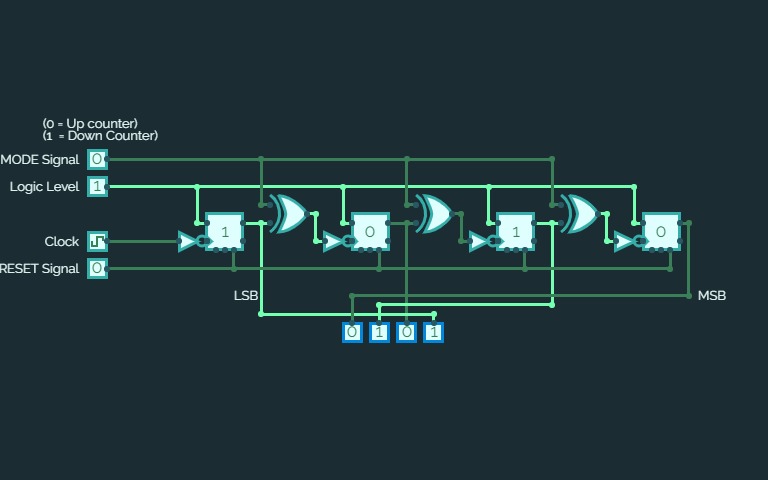
Flip Flop VerificationsAsynchronous/Ripple 4 Bit Up/Down Counter
Asynchronous/Ripple 4 Bit Up/Down CounterAsynchronous/Ripple 4 Bit Up/Down Counter using 4 T Flip Flops sensitive to falling edge of the Clock with a MODE signal and a RESET signal.
Low MODE signal is Up Counting.
High MODE signal is Down Counting.
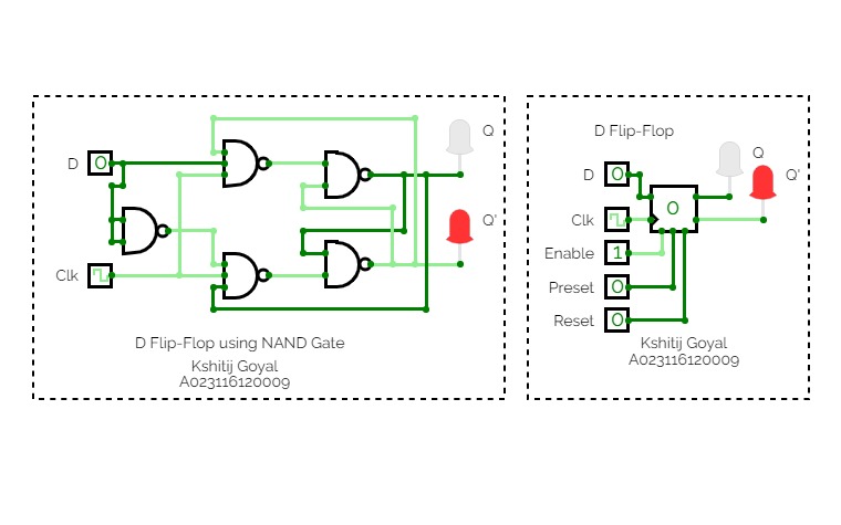
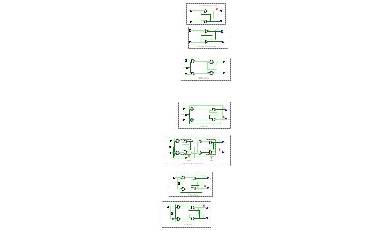
Flip Flop Using NAND GATE
Flip Flop Using NAND GATEFlip Flop Using NAND GATE
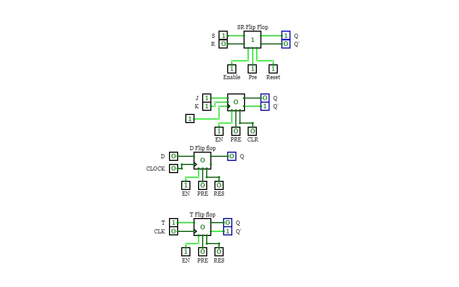
SR, JK, D, T Flip Flop
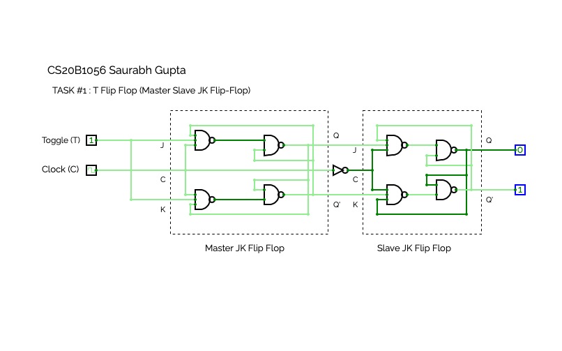
T Flip Flop (Master Slave JK Flip Flop)
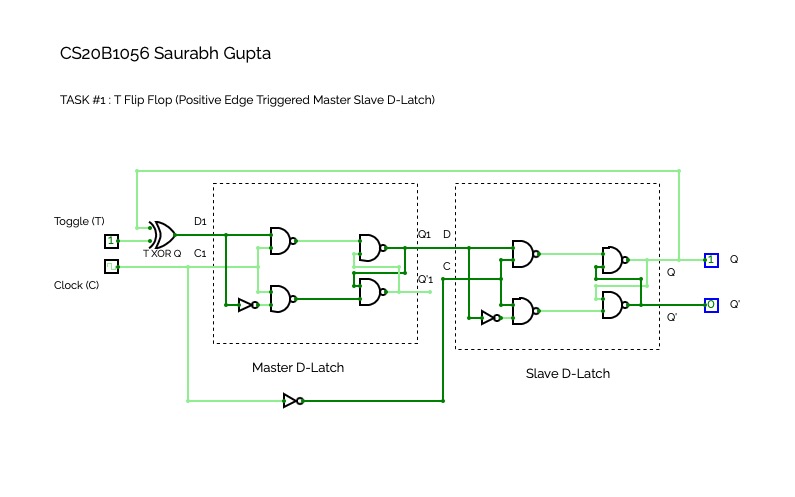
T Flip Flop (Master Slave JK Flip Flop)T Flip Flop (Positive Edge Triggered Master Slave D-Latch)
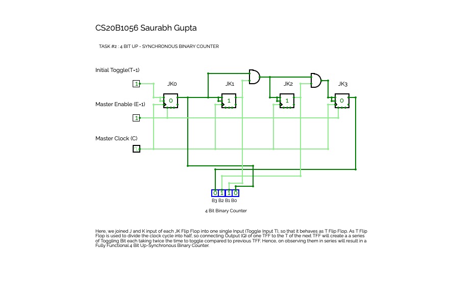
T Flip Flop (Positive Edge Triggered Master Slave D-Latch)4 Bit Up-Synchronous Binary Counter
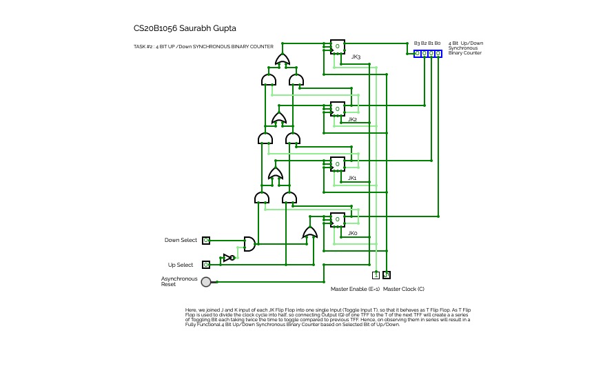
4 Bit Up-Synchronous Binary Counter4 Bit Up/Down Synchronous Binary Counter
4 Bit Up/Down Synchronous Binary CounterECL Lab 5
ECL Lab 5SR Flip-Flop:-
The SR flip-flop, also known as a SR Latch, can be considered as one of the most basic sequential logic circuit possible. This simple flip-flop is basically a one-bit memory bistable device that has two inputs, one which will “SET” the device (meaning the output = “1”), and is labelled S and one which will “RESET” the device (meaning the output = “0”), labelled R.
The Basic SR Flip-flop:-
Truth Table for this Set-Reset Function:-
StateSRQQDescriptionSet1001Set Q » 11101no changeReset0110Reset Q » 01110no changeInvalid0011Invalid Condition
Diagram formed using simulator:-

JK Flip-Flop:-
The JK flip flop is basically a gated SR flip-flop with the addition of a clock input circuitry that prevents the illegal or invalid output condition that can occur when both inputs S and R are equal to logic level “1”. Due to this additional clocked input, a JK flip-flop has four possible input combinations, “logic 1”, “logic 0”, “no change” and “toggle”.
The Basic JK Flip-flop:-
The Truth Table for the JK Function:-
same asfor theSR LatchClockInputOutputDescriptionClkJKQQX0010Memoryno changeX0001‾↓ ̲0110Reset Q » 0X0101‾↓ ̲1001Set Q » 1X10¹⁰toggleaction‾↓ ̲1101Toggle‾↓ ̲1110
Diagram formed using simulator:-

T Flip-Flop:-
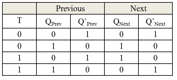
T flip – flop is also known as “Toggle Flip – flop”. To avoid the occurrence of intermediate state in SR flip – flop, we should provide only one input to the flip – flop called Trigger input or Toggle input (T). Then the flip – flop acts as a Toggle switch. Toggling means ‘Changing the next state output to complement of the present state output’.
The Basic T Flip-flop:-
Truth Table of T flip – flop:-
Diagram formed using simulator:-

D Flip-Flop:-
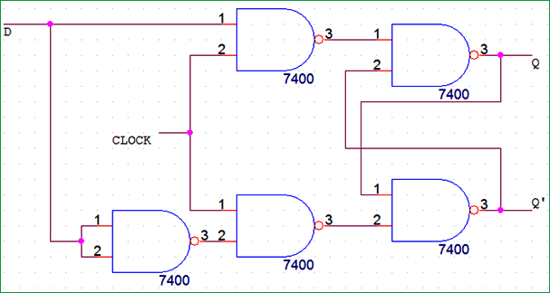
D Flip-flops are used as a part of memory storage elements and data processors as well. D flip-flop can be built using NAND gate or with NOR gate. Due to its versatility they are available as IC packages. The major applications of D flip-flop are to introduce delay in timing circuit, as a buffer, sampling data at specific intervals. D flip-flop is simpler in terms of wiring connection compared to JK flip-flop.
Representation of D Flip-Flop using Logic Gates:
Truth table of D Flip-Flop:
ClockINPUTOUTPUTDQQ’LOWx01HIGH001HIGH110
Diagram formed using simulator:-

