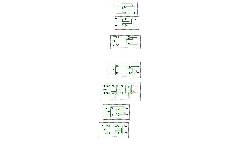

ECL Lab 5
ECL Lab 5SR Flip-Flop:-
The SR flip-flop, also known as a SR Latch, can be considered as one of the most basic sequential logic circuit possible. This simple flip-flop is basically a one-bit memory bistable device that has two inputs, one which will “SET” the device (meaning the output = “1”), and is labelled S and one which will “RESET” the device (meaning the output = “0”), labelled R.
The Basic SR Flip-flop:-

Truth Table for this Set-Reset Function:-
StateSRQQDescriptionSet1001Set Q » 11101no changeReset0110Reset Q » 01110no changeInvalid0011Invalid Condition
Diagram formed using simulator:-

JK Flip-Flop:-
The JK flip flop is basically a gated SR flip-flop with the addition of a clock input circuitry that prevents the illegal or invalid output condition that can occur when both inputs S and R are equal to logic level “1”. Due to this additional clocked input, a JK flip-flop has four possible input combinations, “logic 1”, “logic 0”, “no change” and “toggle”.
The Basic JK Flip-flop:-

The Truth Table for the JK Function:-
same asfor theSR LatchClockInputOutputDescriptionClkJKQQX0010Memoryno changeX0001‾↓ ̲0110Reset Q » 0X0101‾↓ ̲1001Set Q » 1X10¹⁰toggleaction‾↓ ̲1101Toggle‾↓ ̲1110
Diagram formed using simulator:-

T Flip-Flop:-
T flip – flop is also known as “Toggle Flip – flop”. To avoid the occurrence of intermediate state in SR flip – flop, we should provide only one input to the flip – flop called Trigger input or Toggle input (T). Then the flip – flop acts as a Toggle switch. Toggling means ‘Changing the next state output to complement of the present state output’.
The Basic T Flip-flop:-

Truth Table of T flip – flop:-
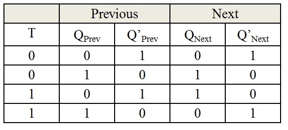
Diagram formed using simulator:-

D Flip-Flop:-
D Flip-flops are used as a part of memory storage elements and data processors as well. D flip-flop can be built using NAND gate or with NOR gate. Due to its versatility they are available as IC packages. The major applications of D flip-flop are to introduce delay in timing circuit, as a buffer, sampling data at specific intervals. D flip-flop is simpler in terms of wiring connection compared to JK flip-flop.
Representation of D Flip-Flop using Logic Gates:

Truth table of D Flip-Flop:
ClockINPUTOUTPUTDQQ’LOWx01HIGH001HIGH110
Diagram formed using simulator:-


