D Flip-Flop
D Flip-FlopLab 10-2
Lab 10-2Flip-Flops using NAND Gate
Flip-Flops using NAND GateSR Flip-Flop:-
The SR flip-flop, also known as a SR Latch, can be considered as one of the most basic sequential logic circuit possible. This simple flip-flop is basically a one-bit memory bistable device that has two inputs, one which will “SET” the device (meaning the output = “1”), and is labelled S and one which will “RESET” the device (meaning the output = “0”), labelled R.
The Basic SR Flip-flop:-
Truth Table for this Set-Reset Function:-
StateSRQQDescriptionSet1001Set Q » 11101no changeReset0110Reset Q » 01110no changeInvalid0011Invalid ConditionDiagram formed using simulator:-

JK Flip-Flop:-
The JK flip flop is basically a gated SR flip-flop with the addition of a clock input circuitry that prevents the illegal or invalid output condition that can occur when both inputs S and R are equal to logic level “1”. Due to this additional clocked input, a JK flip-flop has four possible input combinations, “logic 1”, “logic 0”, “no change” and “toggle”.
The Basic JK Flip-flop:-
The Truth Table for the JK Function:-
same asfor the
SR LatchClockInputOutputDescriptionClkJKQQX0010Memory
no changeX0001‾↓ ̲0110Reset Q » 0X0101‾↓ ̲1001Set Q » 1X10¹⁰toggle
action‾↓ ̲1101Toggle‾↓ ̲1110
Diagram formed using simulator:-

T Flip-Flop:-
T flip – flop is also known as “Toggle Flip – flop”. To avoid the occurrence of intermediate state in SR flip – flop, we should provide only one input to the flip – flop called Trigger input or Toggle input (T). Then the flip – flop acts as a Toggle switch. Toggling means ‘Changing the next state output to complement of the present state output’.
The Basic T Flip-flop:-
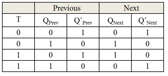
Truth Table of T flip – flop:-
Diagram formed using simulator:-

D Flip-Flop:-
D Flip-flops are used as a part of memory storage elements and data processors as well. D flip-flop can be built using NAND gate or with NOR gate. Due to its versatility they are available as IC packages. The major applications of D flip-flop are to introduce delay in timing circuit, as a buffer, sampling data at specific intervals. D flip-flop is simpler in terms of wiring connection compared to JK flip-flop.
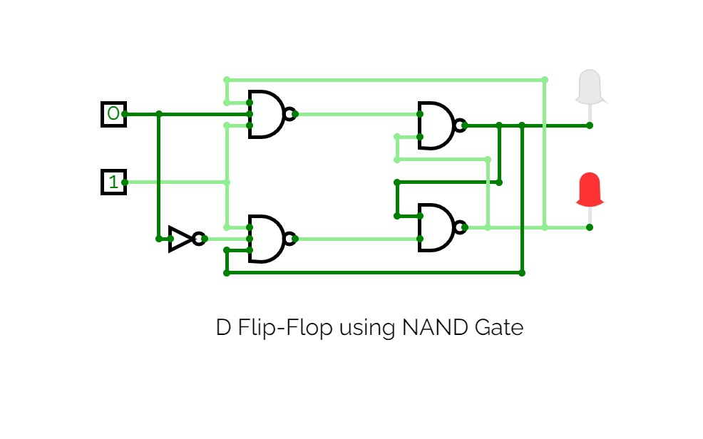
Representation of D Flip-Flop using Logic Gates:
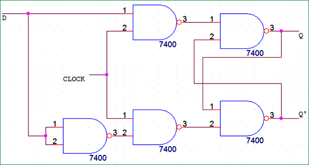
Truth table of D Flip-Flop:
Diagram formed using simulator:-

Traffic Lİght
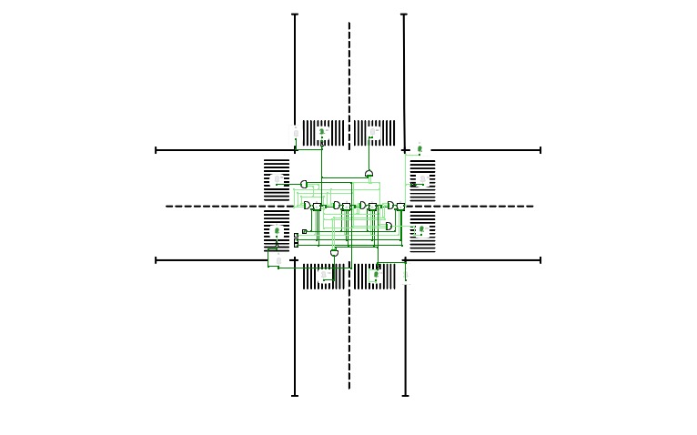
Traffic LİghtDigital Design Project for first semester.
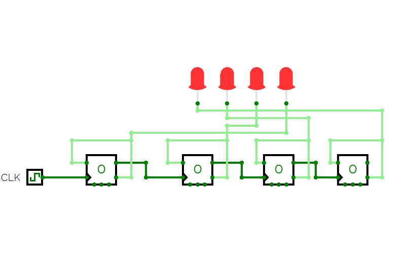
4 Bit Counter with D Flip-Flop
4 Bit Counter with D Flip-FlopPIPO_Register
PIPO_RegisterPedestrian traffic light
Pedestrian traffic lightThis project simulates a pedestrian traffic light based the state of the main traffic light:
-
When the traffic light is red, it is represented as 00
- When it is yellow, it is represented as 10
- When it is green, it is represented as 11
Based on this, it is possible to determine the next state of the pedestrian traffic light (red or green) only taking into account the most significant bit of the main traffic light representation.


