NITIN GUPTA
Member since: 4 years
Educational Institution: Not Entered
Country: Not Entered
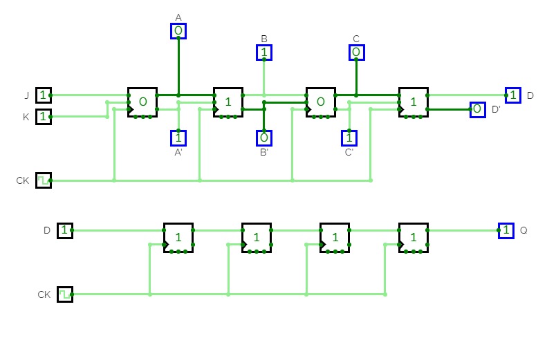
EXP-17
EXP-17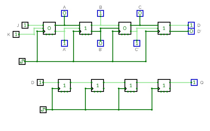
Untitled
Untitled
Untitled
Untitled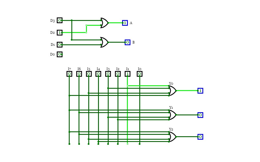
1*8
1*8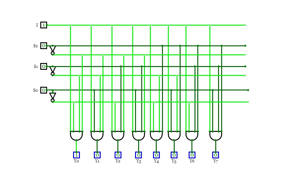
ass2
ass2
Ex-14(A)
Ex-14(A)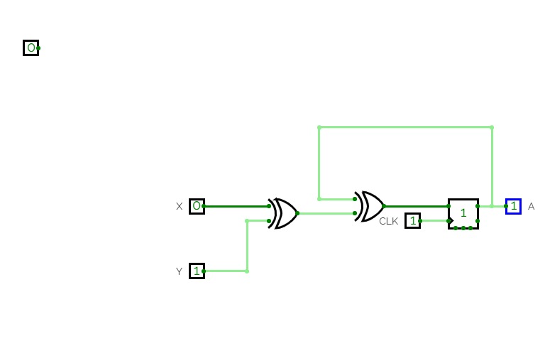
E4
E4
2*2 bit multiplier
2*2 bit multiplier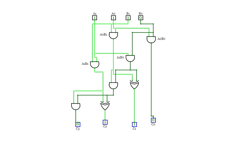
14 B
14 B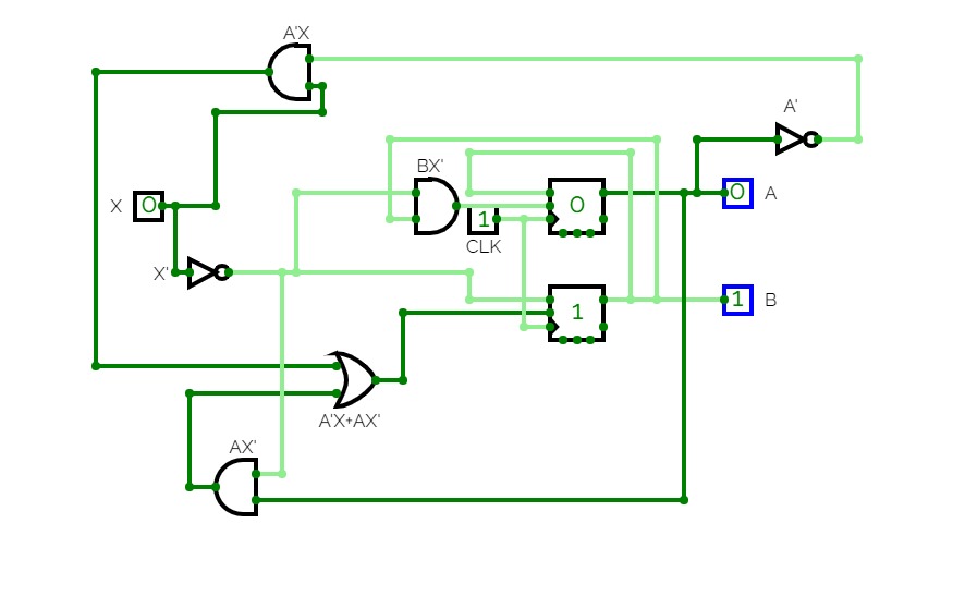
15 B
15 B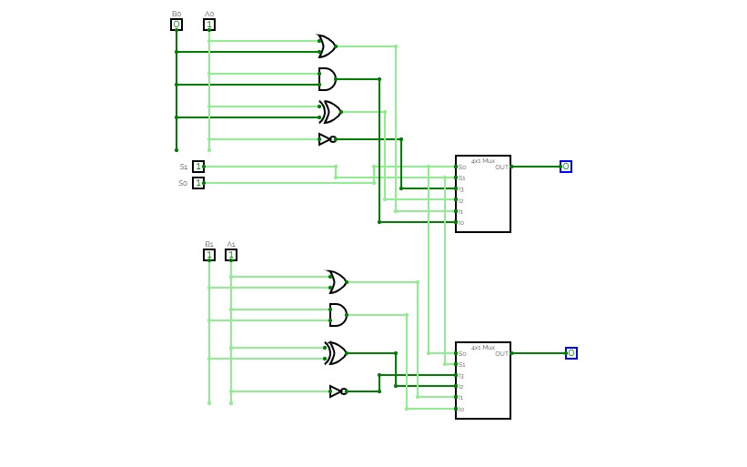
RiGHT Shift
RiGHT Shift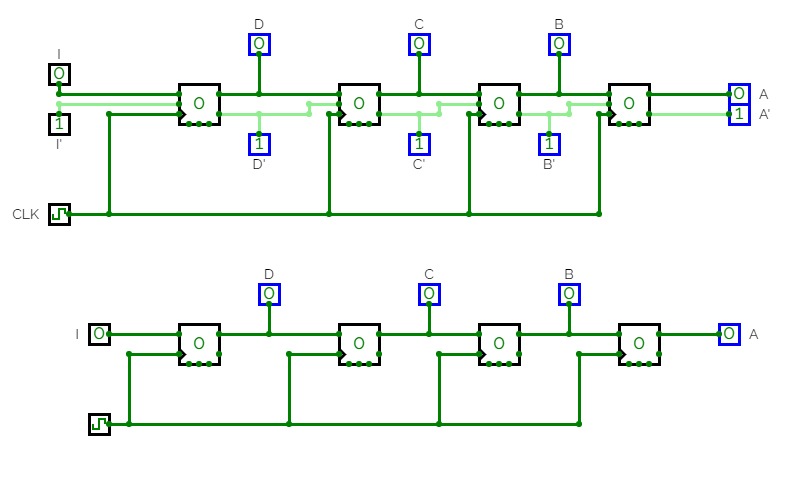
1*4 Demultiplexer
1*4 Demultiplexer
p3
p3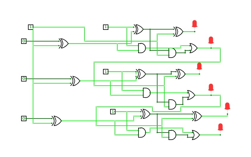
D latch
D latch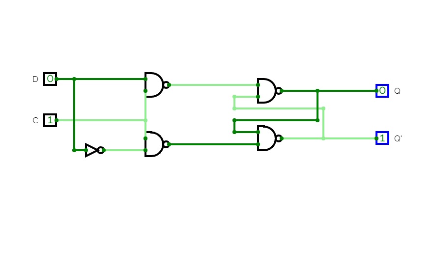
3*3 multiplier
3*3 multiplier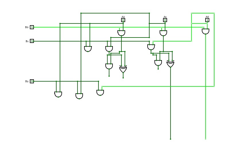
Internal Assesment (3-bit Carry look adder)
Internal Assesment (3-bit Carry look adder)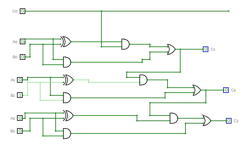
Untitled
Untitled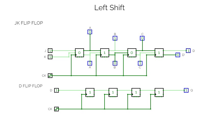
Experiment 1
Experiment 1
EXP4
EXP4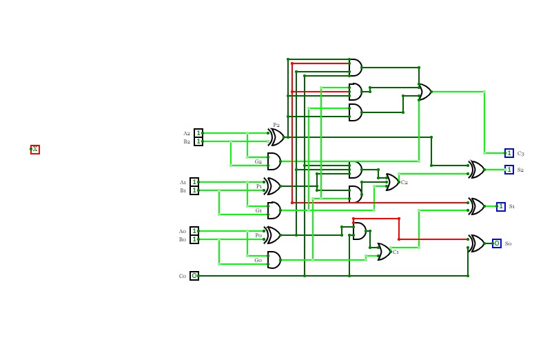
8*1
8*1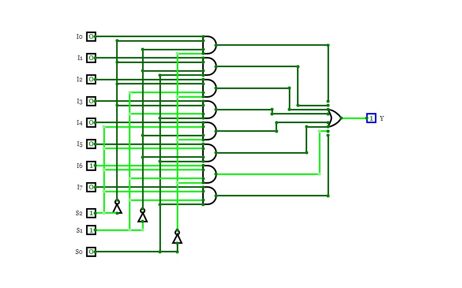
Universal Shift
Universal Shift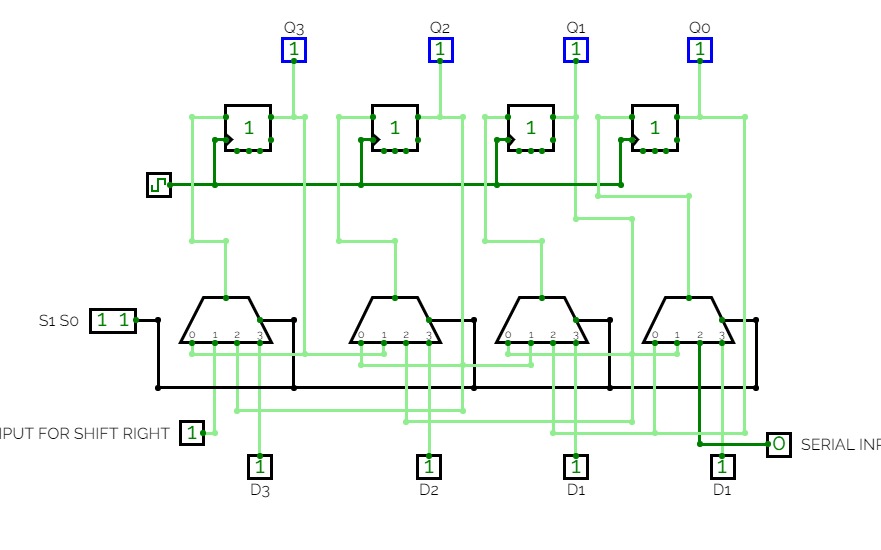
Untitled
Untitled
Untitled
Untitled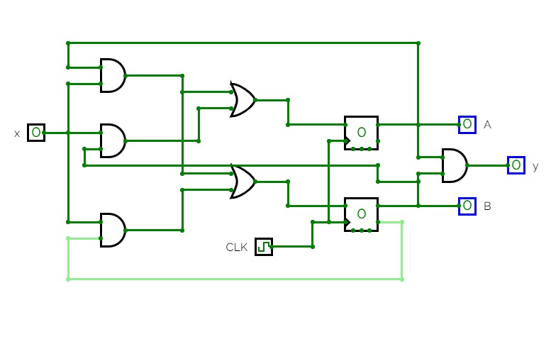
kmap
kmap
1*8
1*8
3*3multiplier
3*3multiplier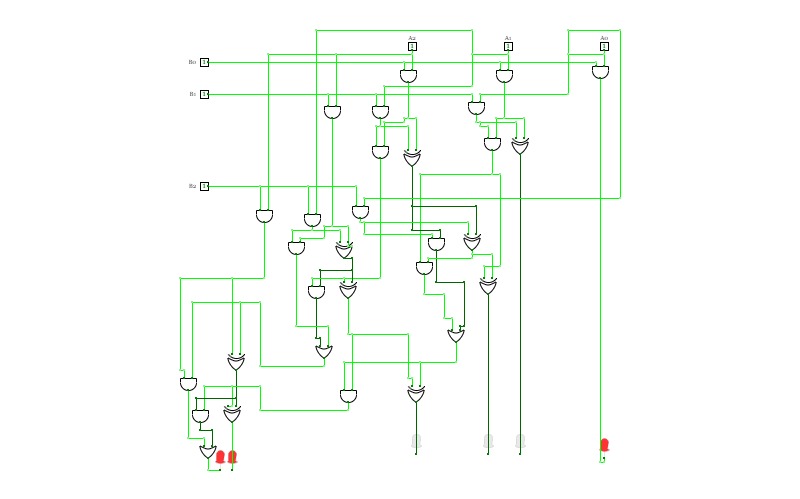
FLIP FLOP
FLIP FLOP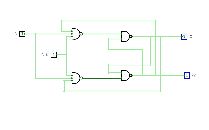
E4
E4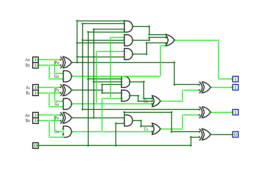
1*8 DEMULTIPLEXER
1*8 DEMULTIPLEXER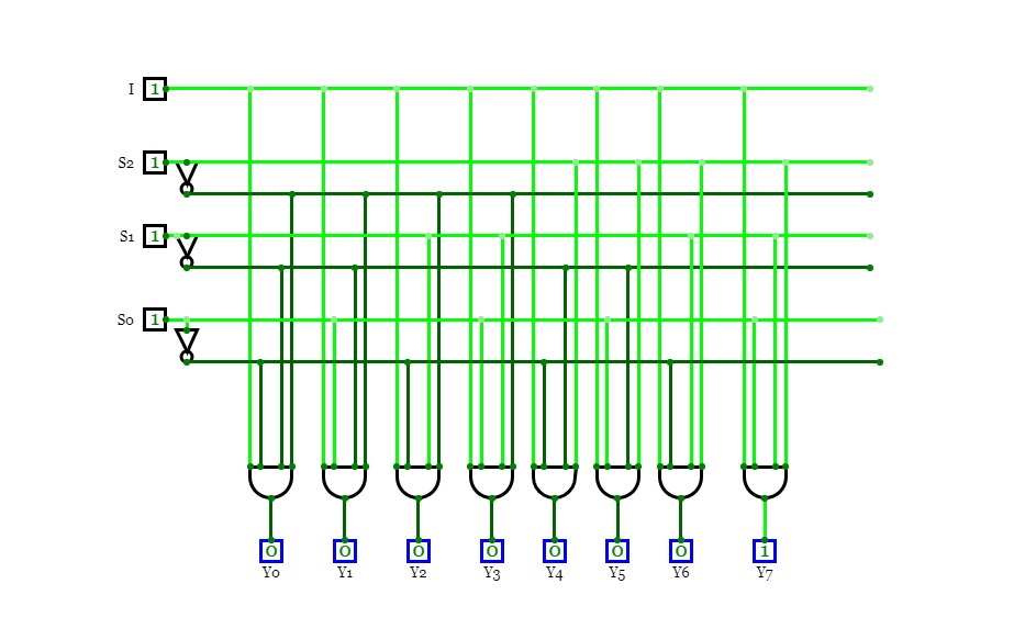
Internal Assesment (3-bit Carry look adder)
Internal Assesment (3-bit Carry look adder)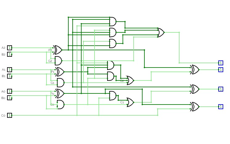
MASTER SLAVE D FILP FLOP
MASTER SLAVE D FILP FLOP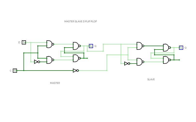
J-K FLIP-FLOP
J-K FLIP-FLOP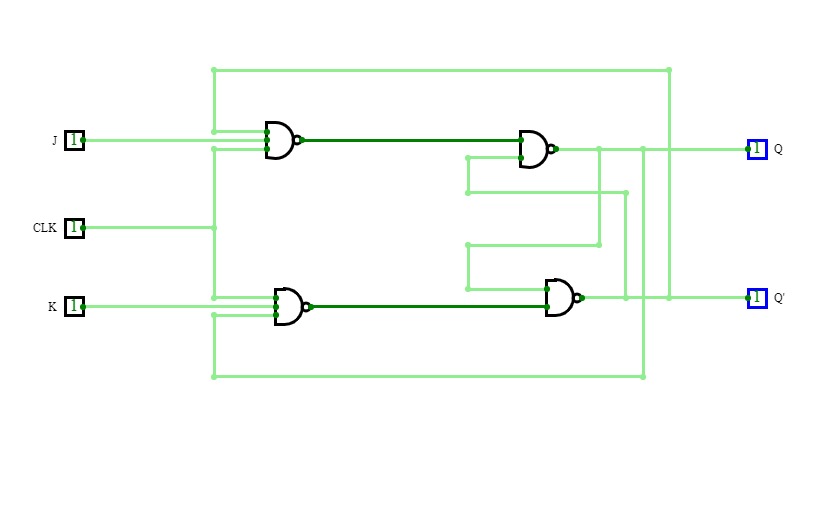
Untitled
Untitled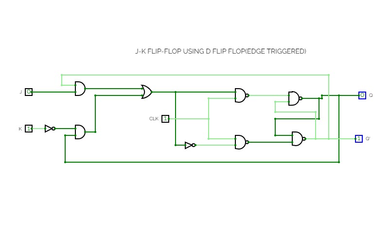
J-K FLIP-FLOP USING D FLIP FLOP(EDGE TRIGGERED)
J-K FLIP-FLOP USING D FLIP FLOP(EDGE TRIGGERED)
ex5
ex5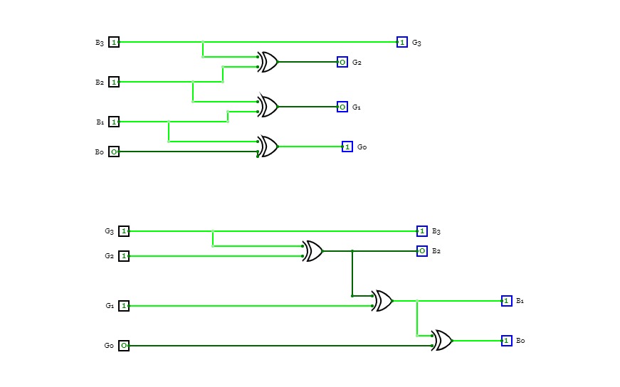
2*4 and 3*8
2*4 and 3*8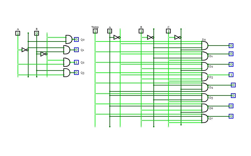
CONTROLLED SR LATCH
CONTROLLED SR LATCH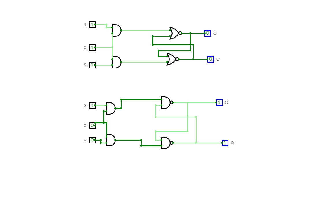
15_A
15_A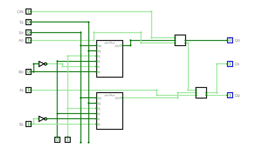
Experiment 1
Experiment 1
J-K FLIP-FLOP
J-K FLIP-FLOP
MULTIPLEXER 4*1 AND 8*1
MULTIPLEXER 4*1 AND 8*1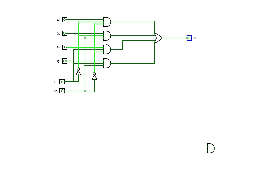
D latch
D latch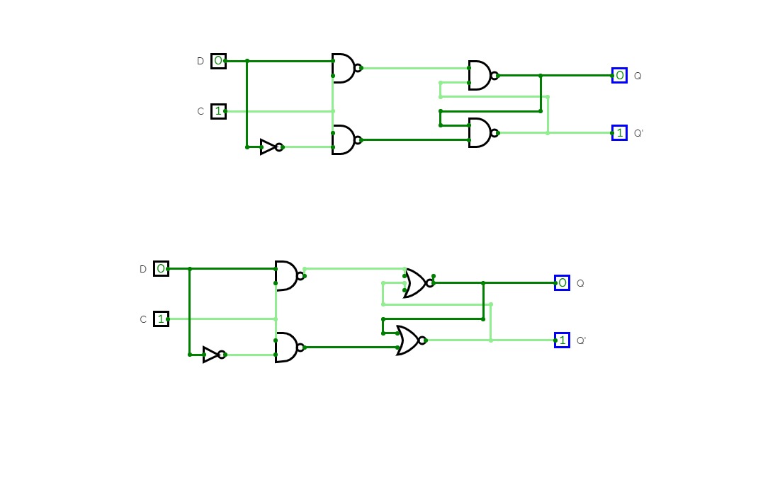
Design of Clocked sequenctial circuit to detect 3 or more consequetive 1s
Design of Clocked sequenctial circuit to detect 3 or more consequetive 1s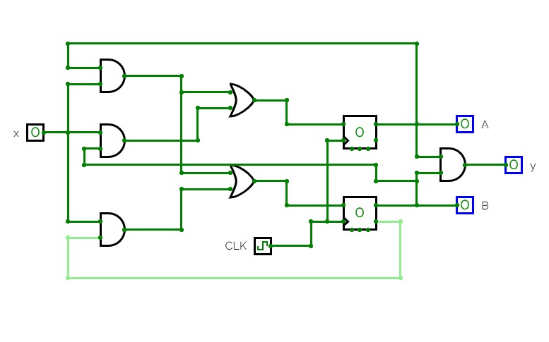
SR LATCH
SR LATCH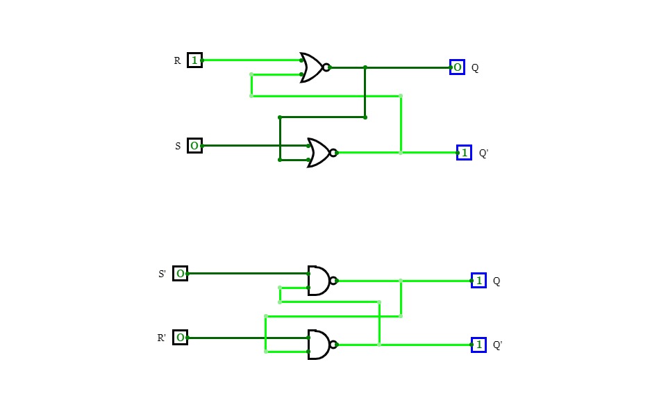
TIMING DIAGRAM 26J-K FLIP-FLOP USING D FLIP FLOP(EDGE TRIGGERED)
TIMING DIAGRAM 26J-K FLIP-FLOP USING D FLIP FLOP(EDGE TRIGGERED)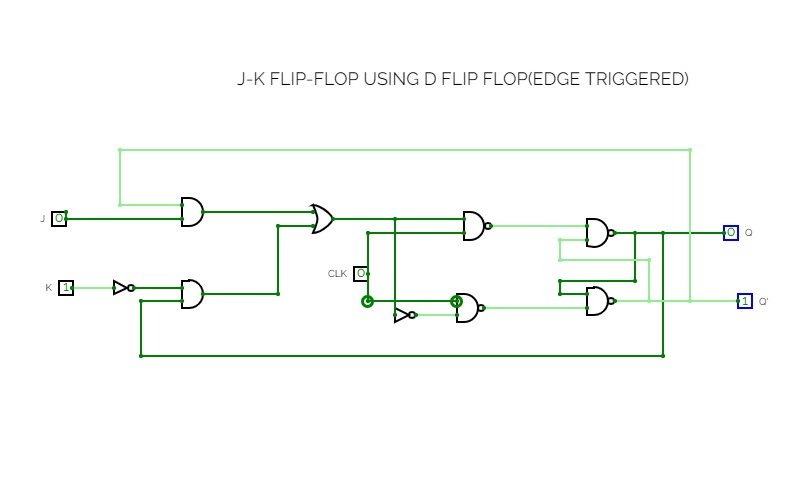
1*4 Demultiplexer
1*4 Demultiplexer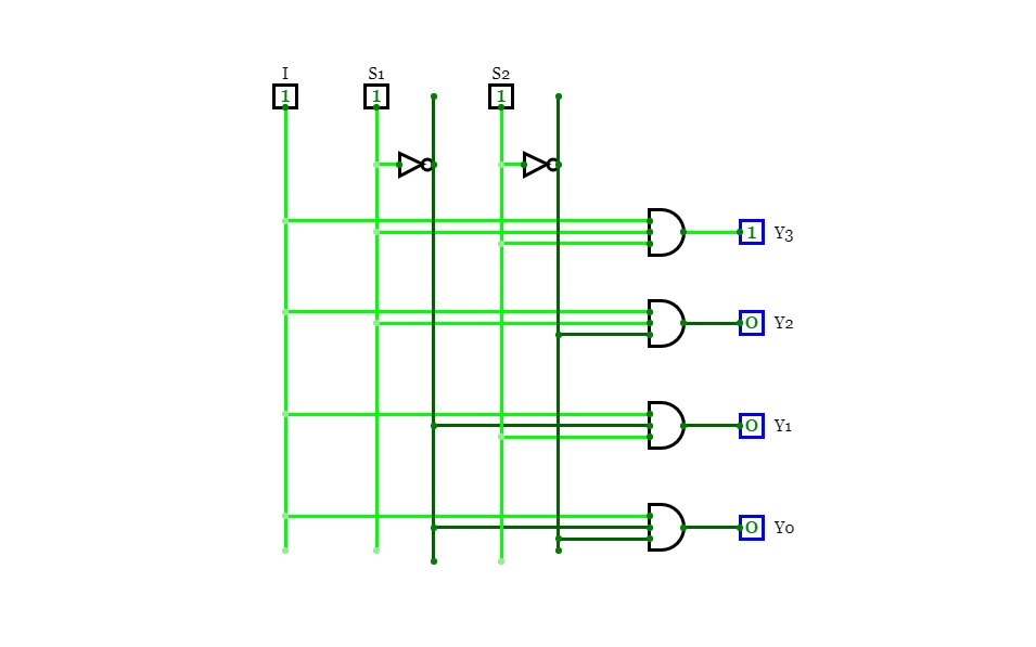
Untitled
Untitled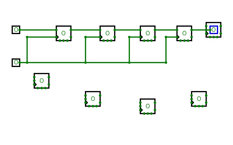
Design of Clocked sequenctial circuit to detect 3 or more consequetive 1s
Design of Clocked sequenctial circuit to detect 3 or more consequetive 1s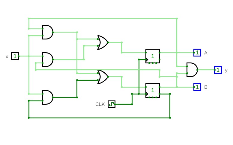
EX 16
EX 16
Left Shift
Left Shift