RAHUL NAHA
Member since: 2 years
Educational Institution: Not Entered
Country: Not Entered
FULL ADDER
FULL ADDER
FULL SUBTRACTOR
FULL SUBTRACTOR
CAT 1 Q1
CAT 1 Q1
2:1 MUX Circuit using SOP Equation -- AOI circuit
2:1 MUX Circuit using SOP Equation -- AOI circuit
NAND21BCE3162
NAND21BCE3162
F'pos21bce3162
F'pos21bce3162
Fnorpos21bce3162
Fnorpos21bce3162
Circuit diagram of 2:1 MUX Circuit using SOP Equation -- NAND circuit:
Circuit diagram of 2:1 MUX Circuit using SOP Equation -- NAND circuit:
task221bce3162
task221bce3162
2:1 MUX Circuit using SOP Equation
2:1 MUX Circuit using SOP Equation
NAND logic circuit of 2:4 Decoder:
NAND logic circuit of 2:4 Decoder:
2: 4 Decoder using 1:2 Decoder:
2: 4 Decoder using 1:2 Decoder:
AOI logic circuit of 2:4 Decoder:
AOI logic circuit of 2:4 Decoder:
2:1 MUX Circuit using POS Equation
2:1 MUX Circuit using POS Equation
NOR21BCE3162
NOR21BCE3162
F'ANDORINV21BCE3162
F'ANDORINV21BCE3162
FNAND 21BCE3162
FNAND 21BCE3162
FULLADDER21BCE3162
FULLADDER21BCE3162
FULLADDSUB21BCE3162
FULLADDSUB21BCE3162
MULTIPLIER21BCE3162
MULTIPLIER21BCE3162
Circuit diagram of 2:1 MUX Circuit using SOP Equation -- AOI circuit
Circuit diagram of 2:1 MUX Circuit using SOP Equation -- AOI circuit
4:1 Mux sl37
4:1 Mux sl37
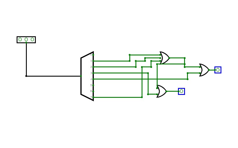
Block diagram for implementing 3 :8 Decoder using 2:4 Decoder:
Block diagram for implementing 3 :8 Decoder using 2:4 Decoder:
4:1 MUX USING 2:1 MUX
4:1 MUX USING 2:1 MUX
Untitled
Untitled
2:1 MUX Circuit using POS Equation
2:1 MUX Circuit using POS Equation
Untitled
Untitled
NAND logic circuit of 4:2 encoder:
NAND logic circuit of 4:2 encoder:
TFF USING DFF
TFF USING DFF
1bit alu
1bit alu
TFLIPFLOPUSINGDFLIPFLOP
TFLIPFLOPUSINGDFLIPFLOP
CAT Q3
CAT Q3
CAT 1 Q4
CAT 1 Q4
CAT1 Q4
CAT1 Q4
CAT 1 Q5
CAT 1 Q5
CAT 1 Q5
CAT 1 Q5
Common Cathode with dc
Common Cathode with dc
Common Cathode with Don't care
Common Cathode with Don't care
Common Cathode with Don'T Care
Common Cathode with Don'T Care
Common Anode w/o dc
Common Anode w/o dc
Common Anode w/o dc
Common Anode w/o dc
Common Cathode without dc
Common Cathode without dc
Common Anode with DC
Common Anode with DC
Common Anode with DC
Common Anode with DC
Common Cathode with Don't care
Common Cathode with Don't care
Common Cathode with Don't care
Common Cathode with Don't care
Common Cathode without dc
Common Cathode without dc
Common Cathode without dc
Common Cathode without dc
da1_q8
da1_q8
da1_q8
da1_q8
da_1_q9
da_1_q9
darn_1_q9
darn_1_q9
da_1_q_10
da_1_q_10
darn_1_q_10
darn_1_q_10
BCD ripple counter
BCD ripple counter
BCD ripple counter
BCD ripple counter
Universal Shift Register
Universal Shift Register
Universal Shift Register
Universal Shift Register
Mealy Machine
Mealy Machine
Mealy Machine
Mealy Machine
4-bit Magnitude comparator
4-bit Magnitude comparator
Moore Machine
Moore Machine
Moore Machine
Moore Machine
4-bit Magnitude comparator
4-bit Magnitude comparator
hotsq2
hotsq2
asynchronous counter
asynchronous counter
asynchronous counter
asynchronous counter
4-Bit Synchronous Up Counter
4-Bit Synchronous Up Counter
CAT 1 Q3
CAT 1 Q3
2:1 MUX Circuit using SOP Equation
2:1 MUX Circuit using SOP Equation
AOI logic circuit of 4:2 encoder:
AOI logic circuit of 4:2 encoder:
Implementation steps for Task I and II using 16:1 Multiplexer Registration Number:
Implementation steps for Task I and II using 16:1 Multiplexer Registration Number:
4-Bit Synchronous Up Counter
4-Bit Synchronous Up Counter
POS21BCE3162
POS21BCE3162
CAT 1 Q1
CAT 1 Q1
Implementation steps for Task I & II using
Implementation steps for Task I & II using


