


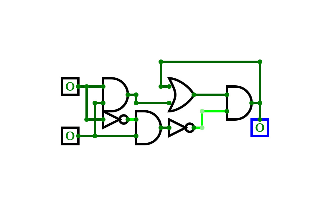

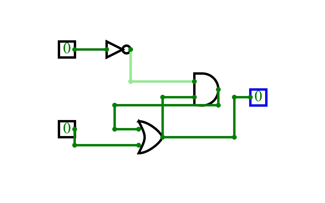
D Flip Flop
D Flip FlopD Flip Flop made from NOT and OR gates
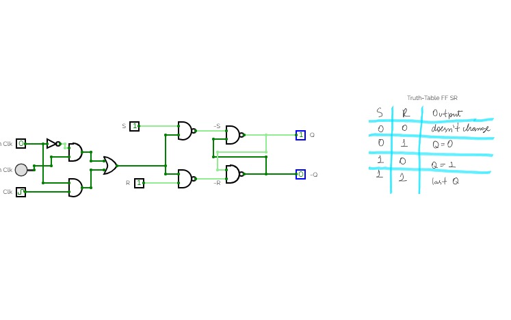

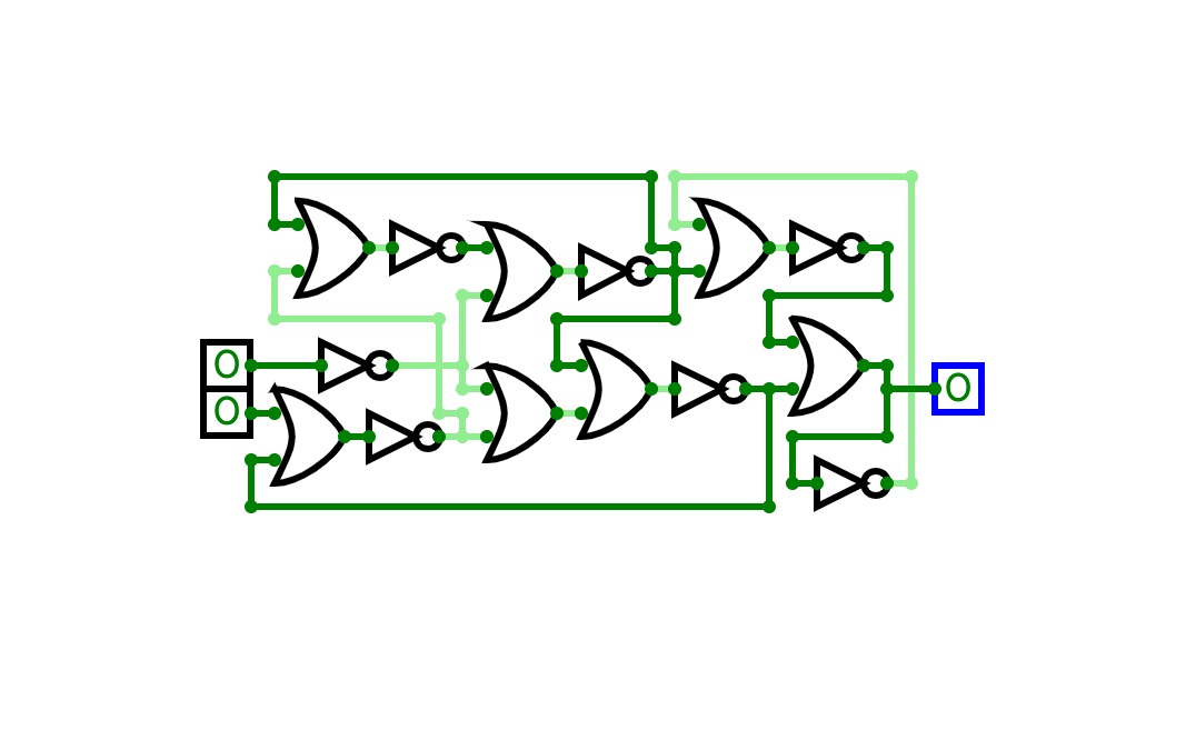
Flip-Flops
Flip-FlopsA flip-flop is a sequential circuit which stores a single bit (binary digit) of data, such data can be used for storage of state. In this project are shown some types of flip-flops.
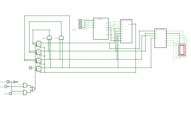
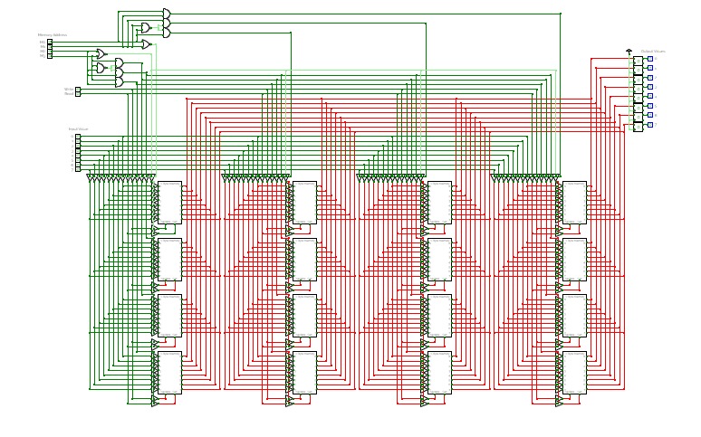
Contador Síncrono_AnnaLu e Filipe
Contador Síncrono_AnnaLu e FilipeTrabalho de Anna Luisa Sá e Filipe, estudantes da UFRJ, para a aula de Circuitos Lógicos ministrada por Pedro Cruz.
Aqui você irá encontrar a primeira versão do nosso contador síncrono, no qual o usuário coloca até quando se deseja contar, ou seja, se ele desejasse contar até 8 números, ele teria que inserir o valor 8 em binário e o contador contaria de 0000 até 0111, e a versão final do trabalho, após a correção de contagem, a qual permite agora o usuário contar até onde ele, de fato, pediu.
Anna Luisa Sá and Filipe Viana's university's project, both of them are students from UFRJ, at Brazil. This project's objective is to count up to fifteen in binary(that is 4 bits) and in here you will find the first version and the final one, which is the official statement for this project.

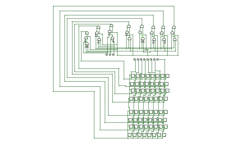
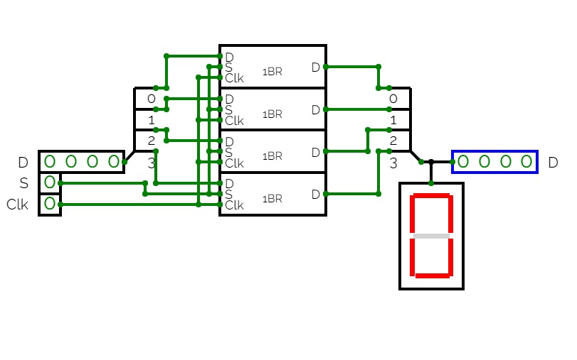
[CSCA] Registers and Memory
[CSCA] Registers and MemoryRegisters and memory elements discussed in the Computer Science and Computer Architectures [CSCA] course at the University of Applied Sciences CAMPUS 02, Graz, Austria.
The project features the following circuits:
- 4-Bit Register - developed by using D flip-flops.
- 4-Bit Register (Enabling the Clock Signal) - 4-Bit Register with enabling of the register implemented via enabling of the clock signal.
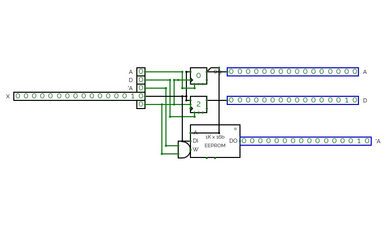
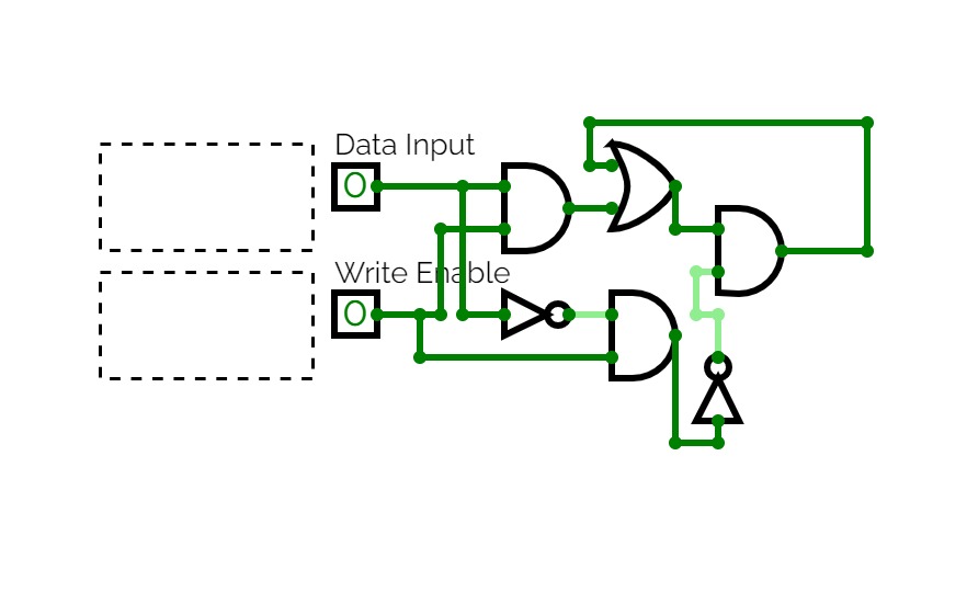
- 4x4-Bit Memory - with read and write access and reading buffer set to zeros in case of writing.
- Tri-State Buffers - explains the tri-state buffer element.
-
Mutually Exclusive Tri-State Buffers - demonstrates how to use tri-state buffers to mutually exclude parts of a circuit.
- 4x4-Bit Memory with Tri-State Buffers - developed by extending the 4x4-Bit Memory with Tri-state buffers to cut of the reading buffer in case of writing.
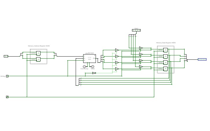
- 4x4-Bit Memory with MAR and MDR - developed by extending the 4x4-Bit Memory with Tri-State Buffers with the Memory Address Register (MAR) and Memory Data Register (MDR).
- 4x4-Bit Random Access Memory (RAM) - demonstrates using the built-in RAM element.
-
4x4-Bit Random Access Memory (RAM) with MAR and MDR - demonstrates using the built-in RAM element extended with the Memory Address Register (MAR) and Memory Data Register (MDR).
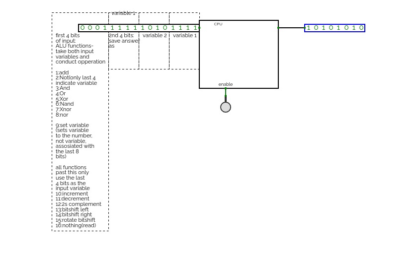
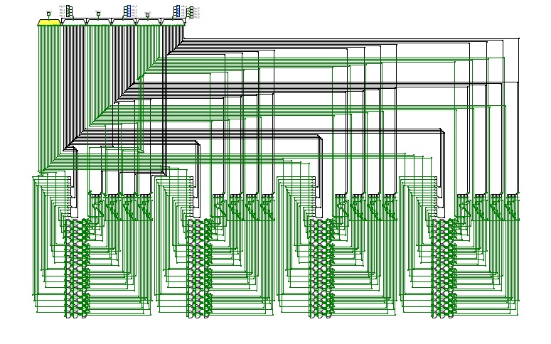
A CPU! this took me a while to figure out, mostly how to get it to run comands, but I eventually found a solution of using 4 bits as function indicators, 4 as where to save the output, 4 as the 2nd input, and 4 as the first input!

Gated-Latch
Gated-LatchA simple Gated-Latch system.


